Semiconductor memory device allowing reliable repairing of a defective column

a memory device and semiconductor technology, applied in the field of semiconductor memory devices, can solve the problems of increasing the chip area, increasing the time required for programming for the repair of defective columns, and increasing the time required for repairing defective columns

Inactive Publication Date: 2001-01-23
MITSUBISHI ELECTRIC CORP
View PDF6 Cites 25 Cited by
  • Summary
  • Abstract
  • Description
  • Claims
  • Application Information

AI Technical Summary

Problems solved by technology

In the case where the replacement column address program circuits are provided corresponding to memory blocks BK1-BKn, respectively, such a problem arises that the chip area increases.
Therefore, the circuits for the redundant column programming occupy a large area, and the semiconductor memory device having a high integration density cannot be achieved.
For these reasons, the time required for programming for the defective column repairing increases, and the production efficiency lowers.
However, programming of the defective column address cannot be performed for the respective memory blocks BK1-BKn.
This significantly reduces the flexibility in programming of a defective column add

Method used


Image

  • Semiconductor memory device allowing reliable repairing of a defective column
  • Semiconductor memory device allowing reliable repairing of a defective column
  • Semiconductor memory device allowing reliable repairing of a defective column

Examples


Embodiment Construction

]

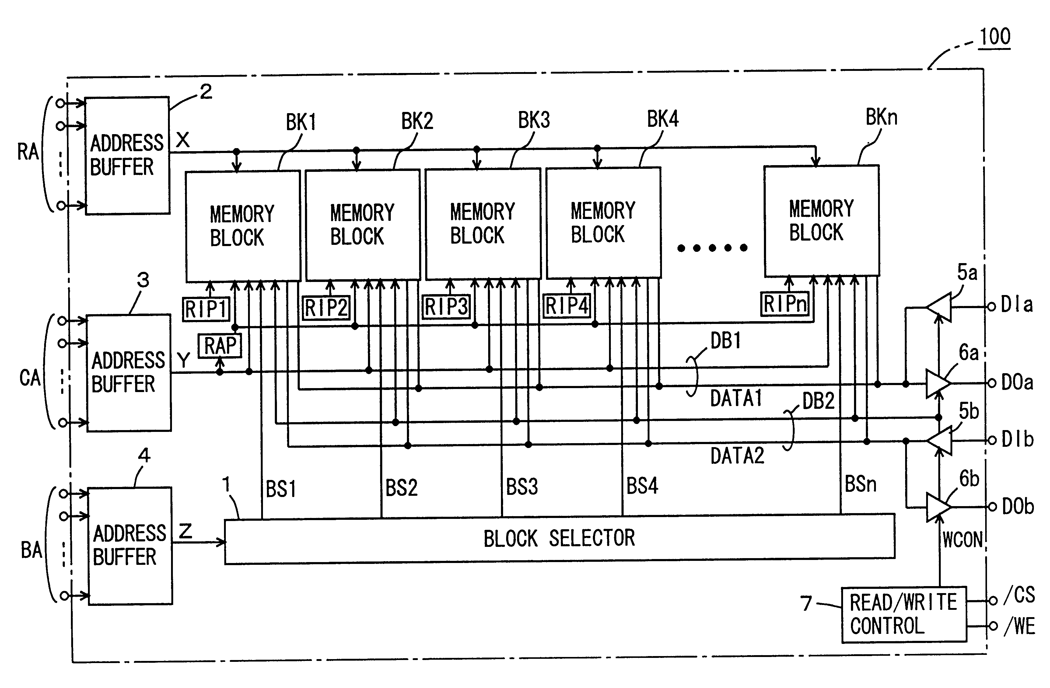
The SRAM has been described as an example of the semiconductor memory device. However, the invention can be applied to various structures provided that the memory block is divided into sub-blocks corresponding to data bits, respectively, and redundant columns are used in memory blocks independently. The invention can be likewise applied to another semiconductor memory device such as a DRAM or a flash memory.

According to the first to eighth embodiments described above, the memory block is divided into memory sub-blocks corresponding to the internal data line pairs. However, the memory sub-blocks may be dispersed in one memory block. For example, such a structure may be employed that one column select line selects the columns corresponding to the respective internal data bits.

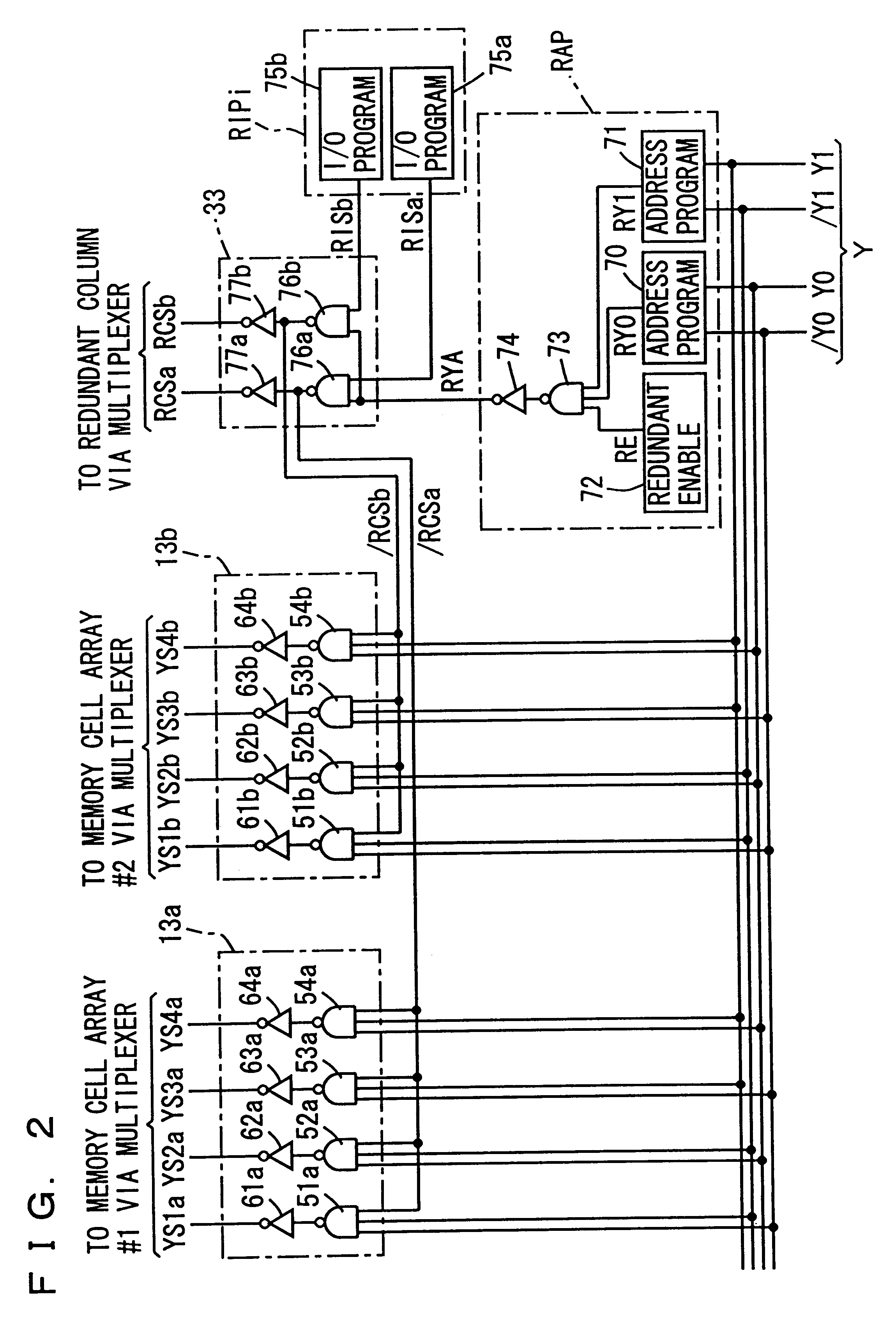
According to the invention, as described above, the replacement IO program circuits are provided corresponding to the memory blocks, and the redundant column address program circuits are smaller in number than t...


PUM


Abstract

A replacement IO program circuit is provided for each of memory blocks coupled commonly to a data bus of multiple bits, and a replacement column address program circuit is provided for a predetermined number of memory blocks. The state of use of a redundant column can be independently determined in each memory block, and the number of program circuits and the area occupied by the circuits are reduced. A semiconductor memory device includes a defective column repairing circuit allowing efficient use of the redundant column without increasing a chip area.

Description

1. Field of the InventionThe invention relates to a semiconductor memory device, and particularly to a semiconductor memory device including a redundant column for repairing a defective memory cell column by replacement. More particularly, the invention relates to repairing of a defective column in the semiconductor memory device which has a plurality of memory blocks each having a redundant column and performs input / output of multi-bit data.2. Description of the Background ArtConventional semiconductor memory devices such as a static random access memory and a dynamic random access memory, which will be referred to as an "SRAM" and a "DRAM" hereinafter, respectively, includes redundant circuits for improving a product yield. If a defect is present in a memory portion (memory cell array) of a produced semiconductor memory device, this defective memory portion is repaired by the function of the redundant circuit. This redundant circuit usually includes a redundant row for repairing a...

Claims


Application Information

Patent Timeline
IPC IPC(8): G11C29/00G11C29/04
CPCG11C29/808G11C29/846
Inventor HARAGUCHI, YOSHIYUKI
Owner MITSUBISHI ELECTRIC CORP
Why Eureka
Try Eureka