Redundant memory circuit for analog semiconductor memory

a technology of analog semiconductor and memory circuit, which is applied in the field of analog semiconductor memory, can solve the problems of major discontinuity, reduced yield due to defective memory cells, and increased memory capacity

Inactive Publication Date: 2002-09-12
LAPIS SEMICON CO LTD
View PDF0 Cites 23 Cited by
  • Summary
  • Abstract
  • Description
  • Claims
  • Application Information

AI Technical Summary

Problems solved by technology

To lengthen the recording and playback times of audio flash memory chips, memory capacities are being increased, necessitating fabrication processes with increasingly smaller feature sizes, and reduced yields due to defective memory cells have become a problem.
A further cause of differences in the programmed threshold voltage is the gate disturb effect, in which the reading or writing of a memory cell disturbs the threshold voltages programmed into other memory cells on the same word line.
This can cause a major discontinuity in the threshold voltage deviation profile, and can degrade the quality of the reproduced audio signal (the reproduced analog signal).
A further problem is that redundancy replacement is limited to one sector per cell array, so if there are two bad sectors in a cell array, they cannot both be replaced with redundant sectors.
This problem becomes increasingly severe as the size of the cell arrays is increased, adversely affecting production yields of high-capacity analog audio flash memories.

Method used


Image

  • Redundant memory circuit for analog semiconductor memory
  • Redundant memory circuit for analog semiconductor memory
  • Redundant memory circuit for analog semiconductor memory

Examples


first embodiment

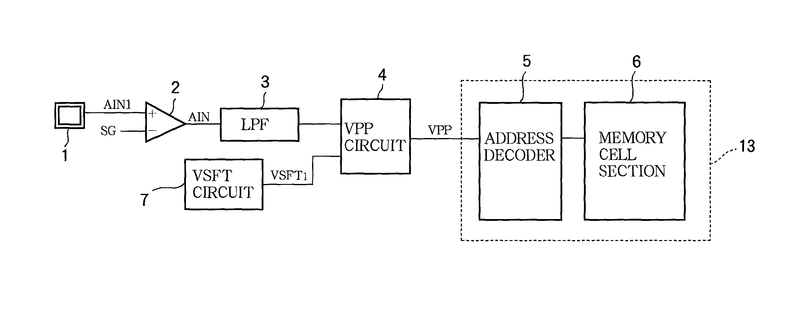
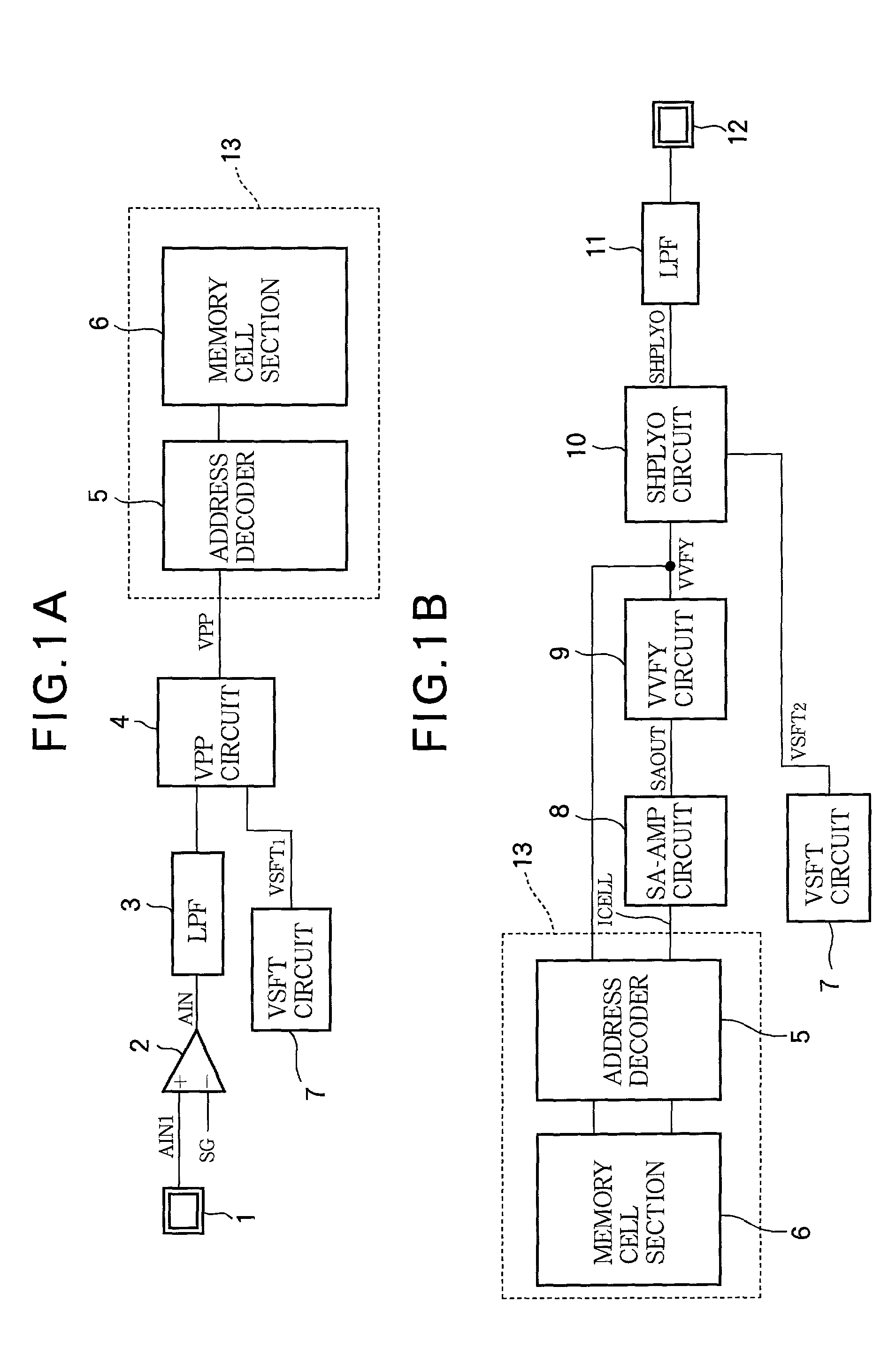
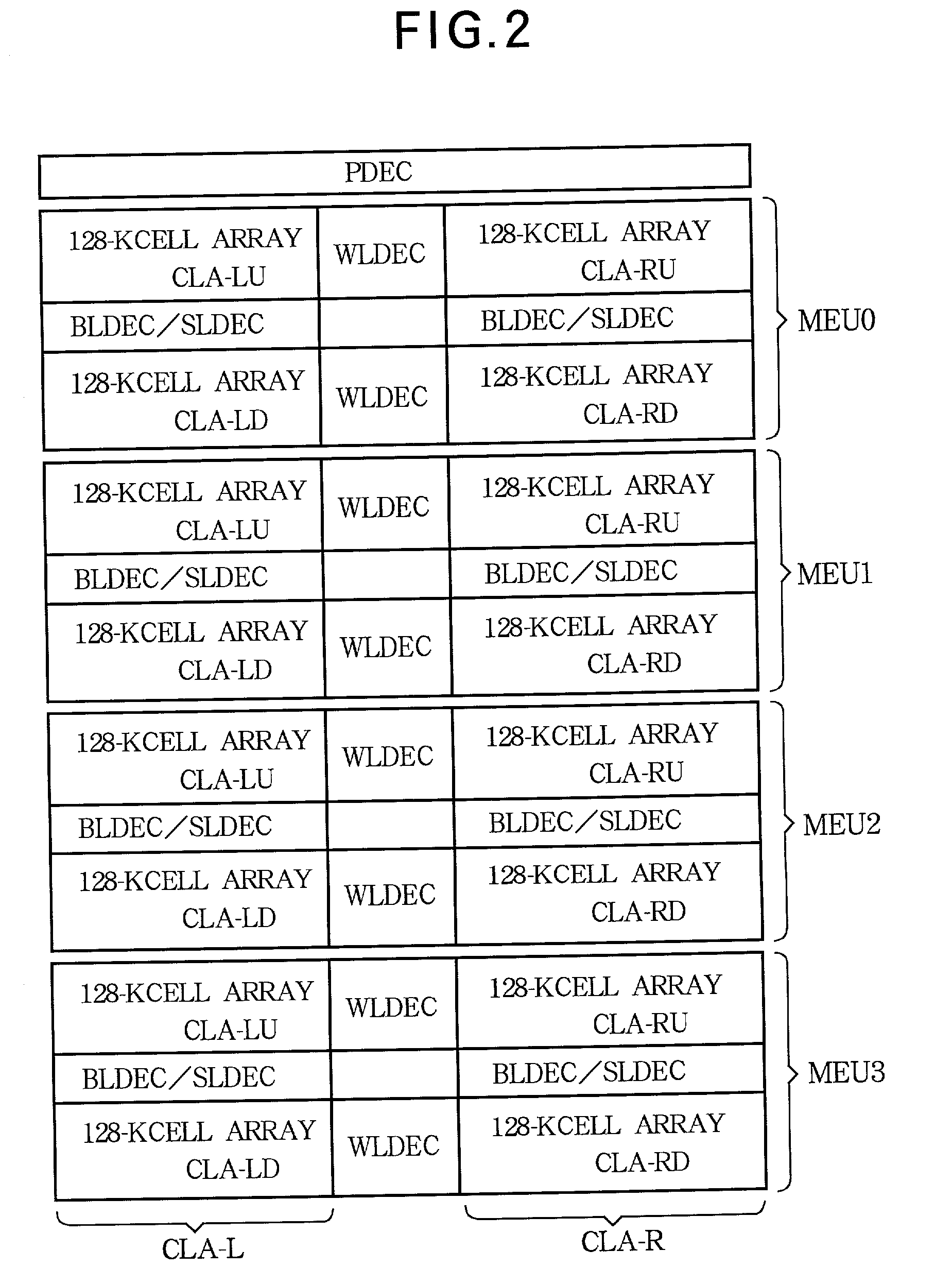
[0206] FIG. 15 shows the layout of the redundant memory circuit of an analog audio flash memory according to the invention. Elements identical to corresponding elements in the non-redundant memory circuit in FIG. 2 are denoted by the same reference characters. The redundant memory circuit in FIG. 15 includes a predecoder PDEC and four memory units AMEU0, AMEU1, AMEU2, AMEU3, an arbitrary one of which will be denoted AMEU below. Hatching is used to denote the positions of redundant sectors in the memory units.

[0207] FIG. 16 shows the layout of a memory unit AMEU in FIG. 15. The memory unit AMEU includes four cell arrays ACLA (ACLA-LU, ACLA-RU, ACLA-LD, ACLA-RD), four word line decoders WLDEC (WLDEC-LU, WLDEC-RU, WLDEC-LD, WLDEC-RD), four bit-line decoders ABLDEC (ABLDEC-LU, ABLDEC-RU, ABLDEC-LD, ABLDEC-RD), and four source line decoders ASLDEC (ASLDEC-LU, ASLDEC-RU, ASLDEC-LD, ASLDEC-RD).

[0208] The sixteen cell arrays ACLA constitute a memory cell section corresponding to the memory ...

second embodiment

[0230] FIG. 20 shows the layout of the redundant memory circuit of an analog audio flash memory according to a second embodiment of the invention. Elements identical to corresponding elements in the non-redundant memory circuit in FIG. 2 are denoted by the same reference characters. The redundant memory circuit in FIG. 20 includes a predecoder PDEC and four memory units BMEU0, BMEU1, BMEU2, BMEU3, an arbitrary one of which will be denoted BMEU below.

[0231] FIG. 21 shows the layout of a memory unit BMEU in FIG. 15. The memory unit BMEU includes four cell arrays BCLA (BCLA-LU, BCLA-RU, BCLA-LD, BCLA-RD), four word line decoders WLDEC (WLDEC-LU, WLDEC-RU, WLDEC-LD, WLDEC-RD), four bit-line decoders BBLDEC (BBLDEC-LU, BBLDEC-RU, BBLDEC-LD, BBLDEC-RD), and four source line decoders BSLDEC (BSLDEC-LU, BSLDEC-RU, BSLDEC-LD, BSLDEC-RD).

[0232] The sixteen cell arrays BCLA constitute a memory cell section corresponding to the memory cell section 6 in FIGS. 1A and 1B. Each cell array BCLA has ...

third embodiment

[0245] FIG. 26 shows the layout of the redundant memory circuit of an analog audio flash memory according to a third embodiment of the invention. Elements identical to corresponding elements in the conventional redundant memory circuit in FIG. 46 are denoted by the same reference characters. The redundant memory circuit in FIG. 26 includes a predecoder PDEC and four memory units CMEU0, CMEU1, CMEU2, CMEU3, an arbitrary one of which will be denoted CMEU below. These memory units add a sector selection circuit SSL to the conventional memory units shown in FIG. 46.

[0246] FIG. 27 shows the layout of a memory unit CMEU in FIG. 26, using the same reference characters for elements identical to corresponding elements in FIG. 47. The memory unit CMEU includes four cell arrays UCLA-LU, UCLA-RU, UCLA-LD, UCLA-RD (an arbitrary one of which will be denoted UCLA), four word line decoders WLDEC (WLDEC-LU, WLDEC-RU, WLDEC-LD, WLDEC-RD), four bit-line decoders UBLDEC (UBLDEC-LU, UBLDEC-RU, UBLDEC-LD...


PUM


Abstract

A redundant memory circuit for use in an analog semiconductor memory has a cell array divided into sectors. To replace bad sectors, the cell array may include a pair of redundant sectors disposed at opposite ends of the cell array, or may have a centrally located redundant sector. Alternatively, the redundant memory circuit may have a sector selection circuit that selects the sectors and redundant sector in sequence from one end of the cell array to the other, or may have a word line selector located in the center of the cell array, or may have two cell arrays and a redundant sector selection circuit that enables a bad sector in one cell array to be replaced by a redundant sector in either of the two cell arrays. These arrangements improve the capability for redundancy replacement and the quality of the reproduced analog signal.

Description

[0001] 1. Field of the Invention[0002] The present invention relates to an analog semiconductor memory such as an analog audio flash memory and, more particularly, to a redundant analog semiconductor memory circuit in which bad sectors are replaced with redundant sectors.[0003] 2. Description of the Related Art[0004] As shown in FIGS. 1A and 1B, an analog audio flash memory comprises an input pad 1, an input amplifier 2, an input low-pass filter (LPF) 3, a write gate voltage generating circuit 4 (known also as a programming voltage generating circuit, referred to below as a VPP circuit), a memory circuit 13 including an address decoder 5 and a memory cell section 6, a shift voltage generating circuit (VSFT circuit) 7, a sense amplifier circuit (SA-AMP circuit) 8, a read gate voltage generating circuit 9 (known also as a verify voltage generating circuit, referred to below as a VVFY circuit), an analog output circuit 10 (known also as a shifted playback output circuit, referred to be...

Claims


Application Information

Patent Timeline
Patent Type & Authority Applications(United States)
IPC IPC(8): G11C16/06G11C29/04G11C16/02G11C27/00G11C7/16G11C16/30G06F12/16G11C29/00G11C16/08G10L19/00
CPCG11C7/16G11C16/08G11C16/30G11C29/816
Inventor SUGIO, KENICHIRO
Owner LAPIS SEMICON CO LTD
Why Eureka
Try Eureka