Organic photosensitive cells having a reciprocal-carrier exciton blocking layer

a photosensitive cell and exciton-blocking technology, which is applied in the field of organic photosensitive optoelectronic devices having exciton-blocking layers, can solve the problems of difficult and expensive production of efficient crystalline-based devices, large surface area, and inability to provide signal or current to control detection circuitry, etc., to achieve good hole injection and minimize recombination losses

Active Publication Date: 2007-06-12
UNIV OF SOUTHERN CALIFORNIA +1
View PDF3 Cites 67 Cited by
  • Summary
  • Abstract
  • Description
  • Claims
  • Application Information

AI Technical Summary

Benefits of technology

[0027]To assure good hole injection, a Fermi level of the cathode is preferably no more than 1 eV higher than the HOMO of the exciton blocking layer. To minimize recombination losses, a HOMO of the exciton blocking layer is preferably no more than 1 eV below the LUMO of the acceptor. An example material for the exciton blocking layer is tris(acetylacetonato) ruthenium(III).

Problems solved by technology

As a general rule, a photovoltaic cell provides power to a circuit, device or equipment, but does not provide a signal or current to control detection circuitry, or the output of information from the detection circuitry.
In contrast, a photodetector or photoconductor provides a signal or current to control detection circuitry, or the output of information from the detection circuitry but does not provide power to the circuitry, device or equipment.
However, efficient crystalline-based devices, especially of large surface area, are difficult and expensive to produce due to the problems inherent in producing large crystals without significant efficiency-degrading defects.
On the other hand, high efficiency amorphous silicon devices still suffer from problems with stability.
The maximum total power generated by a PV device is inherently incapable of exceeding the product, ISC×VOC.
Either of these outcomes is undesirable in a photosensitive optoelectronic device.
Such a process can be induced by the built-in electric field, but the efficiency at the electric fields typically found in organic devices (F˜106 V / cm) is low.
However, some organic PV devices typically have relatively low external quantum efficiency, being on the order of 1% or less.
In this process energy is lost which will result in a lower efficiency for the device.

Method used


Image

  • Organic photosensitive cells having a reciprocal-carrier exciton blocking layer
  • Organic photosensitive cells having a reciprocal-carrier exciton blocking layer
  • Organic photosensitive cells having a reciprocal-carrier exciton blocking layer

Examples


Embodiment Construction

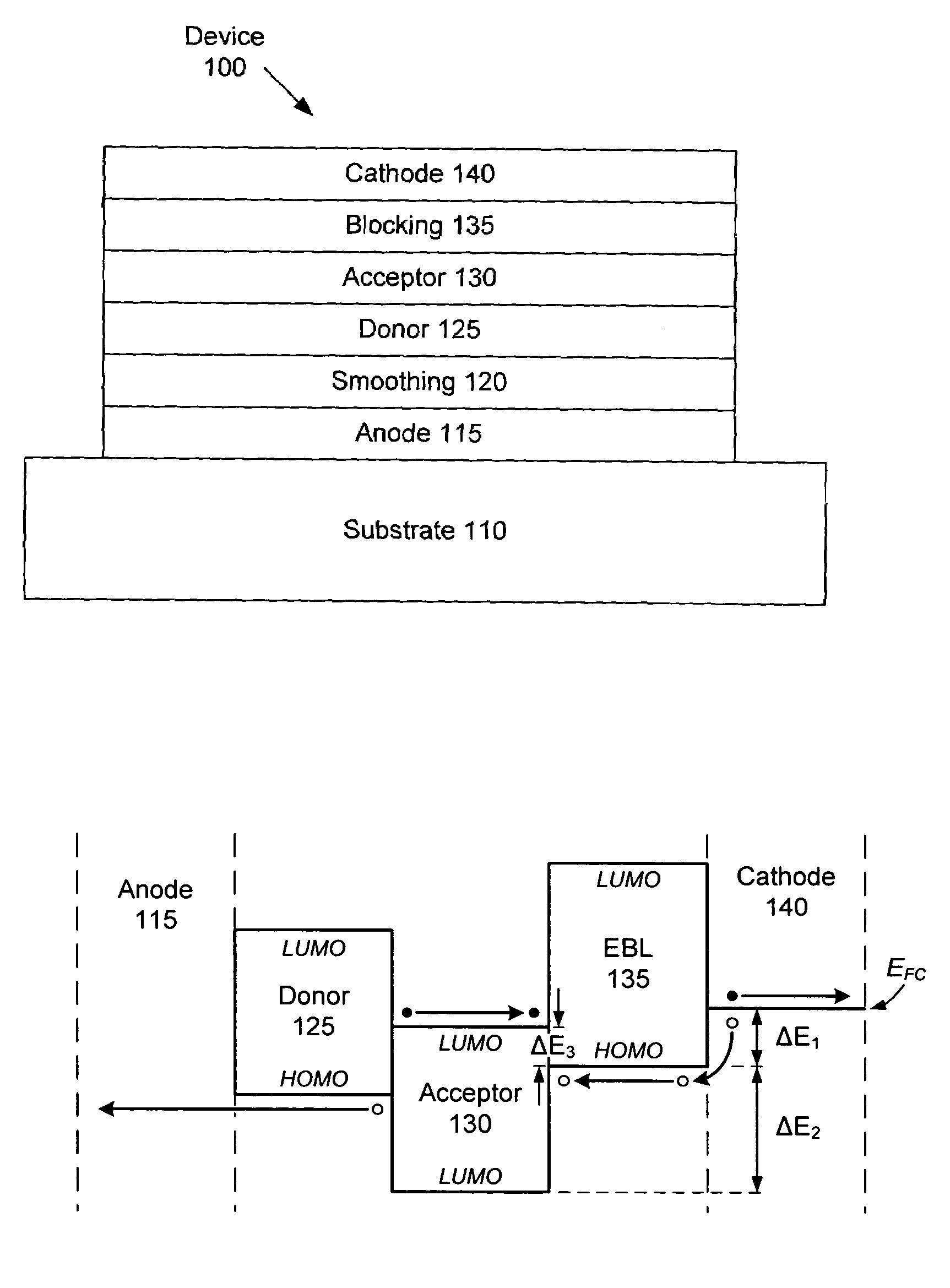
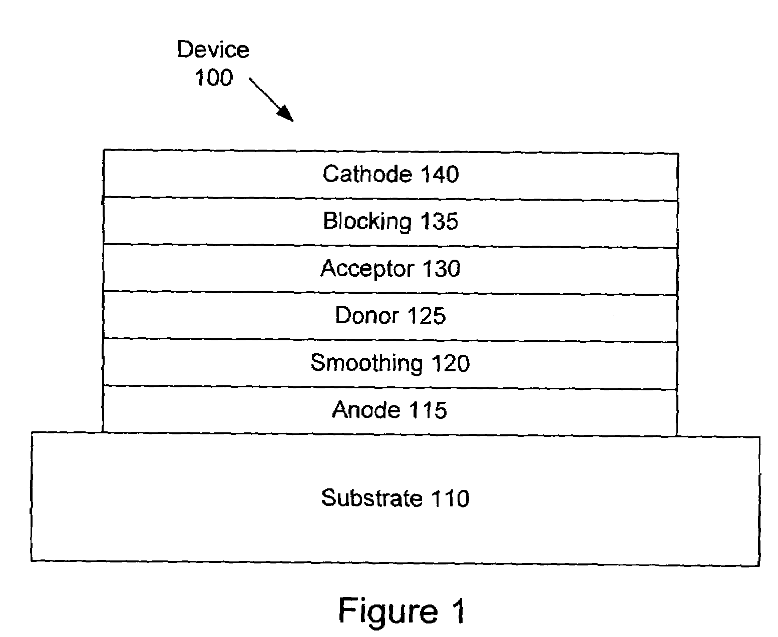
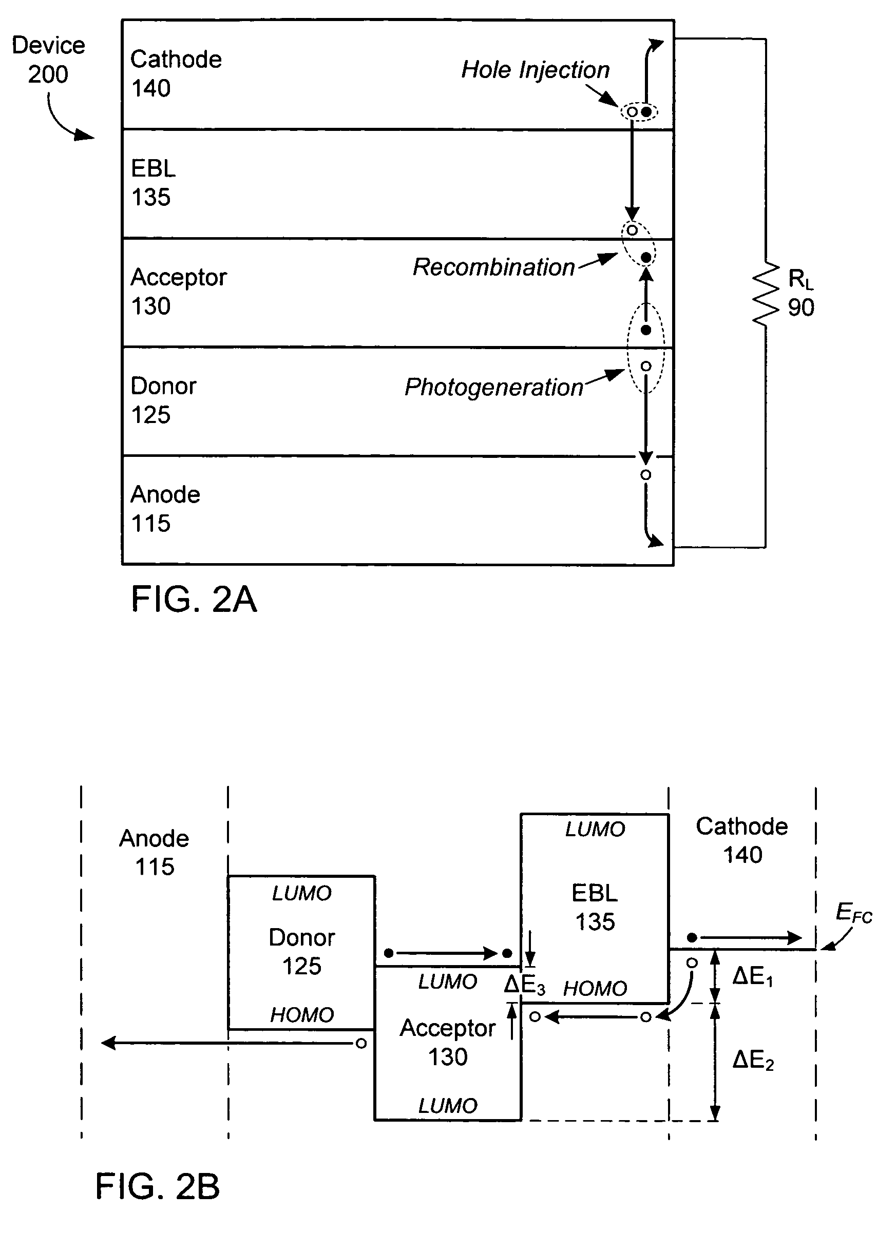
[0047]An organic photosensitive optoelectronic device is provided. Organic devices of embodiments of the present invention may be used, for example, to generate a usable electrical current from incident electromagnetic radiation (e.g., PV devices) or may be used to detect incident electromagnetic radiation. Embodiments of the present invention may comprise an anode, a cathode, and a photoactive region between the anode and the cathode. The photoactive region is the portion of the photosensitive device that absorbs electromagnetic radiation to generate excitons that may dissociate in order to generate an electrical current. Organic photosensitive optoelectronic devices may also include at least one transparent electrode to allow incident radiation to be absorbed by the device. Several PV device materials and configurations are described in U.S. Pat. No. 6,657,378 to Forrest et al., U.S. Pat. No. 6,580,027 to Forrest et al., and U.S. Pat. No. 6,352,777 to Bulovic et al., which are inc...


PUM

PropertyMeasurementUnit
HOMOaaaaaaaaaa
LUMOaaaaaaaaaa
external quantum efficiencyaaaaaaaaaa

Abstract

A photosensitive cell includes an anode and a cathode; a donor-type organic material and an acceptor-type organic material forming a donor-acceptor junction connected between the anode and the cathode; and an exciton blocking layer connected between the acceptor-type organic material of the donor-acceptor junction and the cathode, the blocking layer consisting essentially of a material that has a hole mobility of at least 10−7 cm2 / V-sec or higher, where a HOMO of the blocking layer is higher than or equal to a HOMO of the acceptor-type material.

Description

UNITED STATES GOVERNMENT RIGHTS[0001]This invention was made with U.S. Government support under Contract No. 339-4012 awarded by U.S. Department of Energy, National Renewable Energy Laboratory. The government has certain rights in this invention.JOINT RESEARCH AGREEMENT[0002]The claimed invention was made by, on behalf of, and / or in connection with one or more of the following parties to a joint university corporation research agreement: Princeton University, The University of Southern California, the Universal Display Corporation, and the Global Photonics Energy Corporation. The agreement was in effect on and before the date the claimed invention was made, and the claimed invention was made as a result of activities undertaken within the scope of the agreement.FIELD OF THE INVENTION[0003]The present invention generally relates to organic photosensitive optoelectronic devices. More specifically, it is directed to organic photosensitive optoelectronic devices having an exciton blocki...

Claims


Application Information

Patent Timeline
Patent Type & Authority Patents(United States)
IPC IPC(8): H01L29/08H01L21/00H01L51/40
CPCB82Y10/00H01L51/0086H01L51/4246H01L51/0046H01L51/0062Y02E10/549H01L2251/308H01L51/0078H10K85/211H10K85/649H10K85/311H10K85/344H10K30/211H10K2102/103H10K30/00
Inventor RAND, BARRY P.FORREST, STEPHEN R.THOMPSON, MARK E.
Owner UNIV OF SOUTHERN CALIFORNIA
Why Eureka
Try Eureka