Coupling device for interfacing power amplifier and antenna in differential mode

a power amplifier and differential mode technology, applied in the direction of transmission monitoring, modulation, substation equipment, etc., can solve the problems of increasing component cost, increasing complexity of the entire electronic arrangement, deteriorating signal performance, etc., and achieve the effect of reducing the gain of the amplifier

Inactive Publication Date: 2007-06-26
SEIKO EPSON CORP
View PDF6 Cites 15 Cited by
  • Summary
  • Abstract
  • Description
  • Claims
  • Application Information

AI Technical Summary

Benefits of technology

[0021]It is thus an advantage of the present invention that a differential signal, propagating between the electronic circuit and the antenna, is not influenced by adverse effects of a ground plane which has to be provided in the case of unbalanced lines. Another advantage of not having the balun in accordance with the invention is also that the amplifier gain can be reduced.
[0022]Using completely differential signal paths the return path is not in a ground plane but a signal line. It is advantageous that differences in voltage levels from point to point that deteriorate the signal performance in terms of noise injection are not created. Furthermore, it is an advantage that transmission signal paths from the electronic circuit to the antenna and receiving signal paths from the antenna to the electronic circuit exhibit the same configuration such that the ground plane has no adverse influences. Thus, noise effects can be avoided. Furthermore, losses at the output of a power amplifier can be avoided. Moreover a better signal-to-noise ratio compared to conventional arrangements can be provided. The coupling device for coupling an electronic circuit for at least one antenna unit to exchange signals between the electronic circuit and the at least one antenna unit essentially comprises:
[0023]a) first input / output terminals connected to the electronic circuit by means of a first input / output signal path;
[0024]b) a matching unit coupled to the first input / output terminals by means of a first signal path for performing an impedance matching with respect to the electrical signals;
[0025]c) a filter unit coupled to the output of the matching unit by means of a second signal path for filtering the electrical signals; and
[0026]d) second input / output terminals connected to the filter unit and the at least one antenna unit by means of a second input / output signal path, wherein the signal paths arranged between the electronic circuit and the at least antenna unit are provided completely differential.

Problems solved by technology

A disadvantage of such arrangements is that a balun required to convert the signal path from differential to single ended may deteriorate a signal performance and may increase component costs.
Thus, it is a disadvantage of the conventional arrangement shown in FIG. 4(a) that it is necessary to provide an additional unit between the differential input / output amplifier 122 and a subsequent matching and filter network.
It is a major disadvantage of conventional arrangements using differential input / output amplifiers having differential input lines and differential output lines, and single ended input / output networks following a differential input / output amplifier that a balun unit is required in order to adapt a balanced line to an unbalanced line.
Disadvantageously a balun unit results in an increasing complexity of the entire electronic arrangement and in signal losses caused by the balun unit.
Furthermore, it is a disadvantage of conventional arrangements that an additional component, e.g. the balun unit, has to be provided which increases overall costs.
Another major disadvantage of conventional arrangements using single ended input / output networks connected between a differential amplifier unit and a single ended antenna unit is that currents are injected into a ground plane thus that the injected currents depend on changes in ground equivalence impedance distribution.
This situation may cause differences in voltage levels that deteriorate a signal performance in terms of noise injection.

Method used


Image

  • Coupling device for interfacing power amplifier and antenna in differential mode
  • Coupling device for interfacing power amplifier and antenna in differential mode
  • Coupling device for interfacing power amplifier and antenna in differential mode

Examples


Embodiment Construction

[0055]The present invention now will be described more fully hereinafter with reference to the accompanying drawings, in which preferred embodiments of the invention are shown.

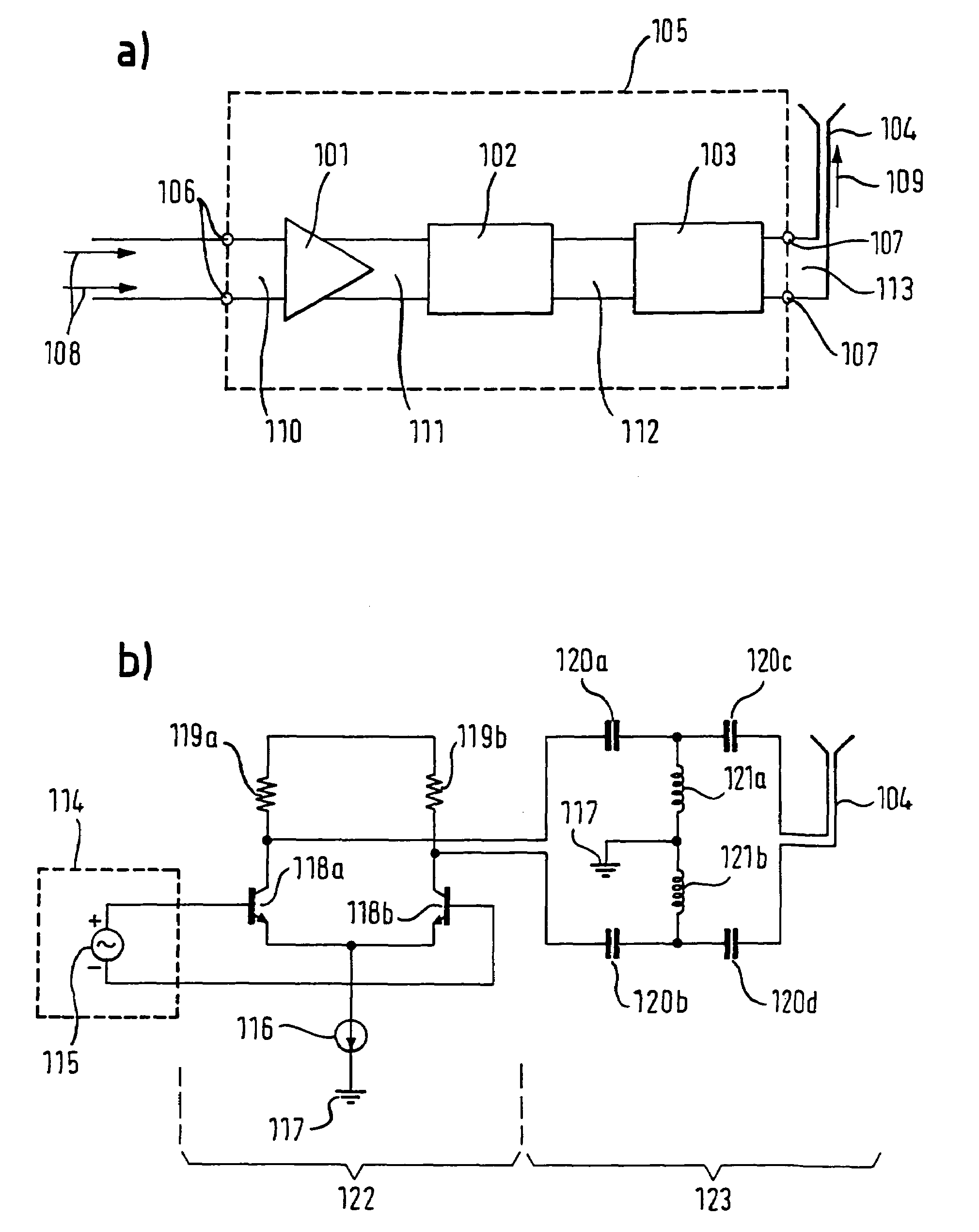
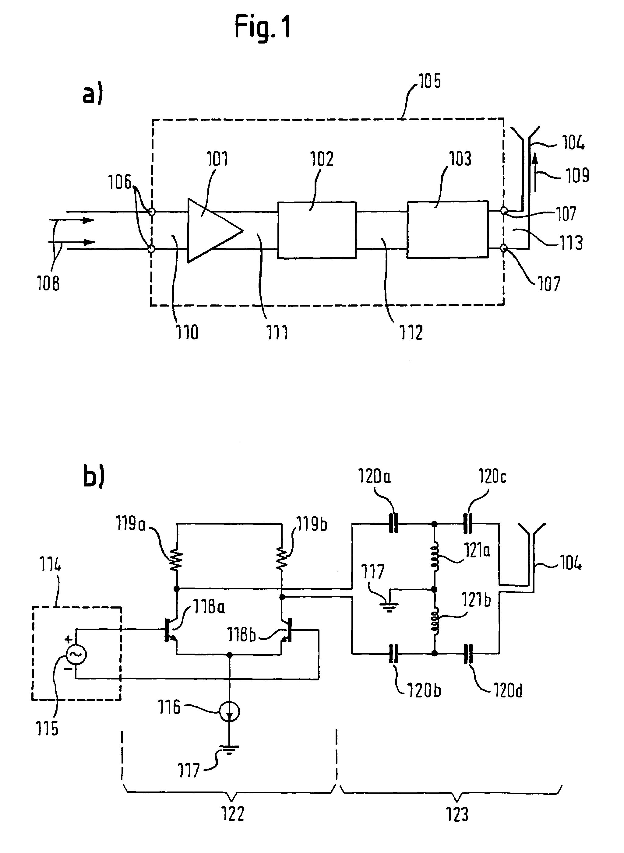
[0056]FIG. 1(a) is a block diagram of a coupling device 105 according to a preferred embodiment of the present invention. The coupling device is designed to couple at least one antenna unit 104 to an electronic circuit 114 (shown in FIG. 1(b) and described below). It is noted that one or more antenna units 104 can be coupled to the coupling device 105 as is appropriate for a given application.

[0057]Furthermore, it is noted that the signal paths can be provided uni-directional from the electronic circuit 114 to the antenna unit 104 as it is shown in the preferred embodiment described with reference to FIG. 1(a) and FIG. 1(b), or the signal paths can be provided uni-directional from the antenna unit 104 to the electronic circuit 114. Furthermore, the signal paths can be provided bi-directional to exchange electr...


PUM


Abstract

A coupling device for coupling an electronic circuit for at least one antenna unit to exchange electrical signals between the electronic circuit and the at least one antenna unit comprises a first input / output signal path, a matching unit coupled to the first input / output signal path, a filter unit coupled to the output of the matching unit by means of a second signal path and a second input / output signal path for connecting the filter unit to the at least one antenna unit, wherein the signal path arranged between the electronic circuit and the at least one antenna unit are provided completely differential.

Description

TECHNICAL FIELD OF THE INVENTION[0001]The present invention relates to the coupling of an electronic circuit to at least one antenna unit in order to exchange electric signals between the electronic circuit and the at least one antenna unit, and in particular to a coupling device for coupling an electronic circuit to at least one antenna unit by means of fully differential signal paths.[0002]In RF (radio frequency) applications an efficient coupling of antenna units to electronic circuits in order to transmit RF signals provided by the electronic circuits or to receive RF signals detected by antenna units is essential. A conventional coupling device arranged between an electronic circuit and an antenna unit comprises, e.g. amplifier units, matching units and filter units. The respective units comprise single ended and / or differential inputs and outputs. Conventionally a power amplifier has to be coupled to an antenna unit having a single ended input.[0003]In case the amplifier unit ...

Claims


Application Information

Patent Timeline
Patent Type & Authority Patents(United States)
IPC IPC(8): H04M1/00H03F3/45H04B1/04
CPCH03F3/45085H04B1/0458H03F2200/541
Inventor CAIRO, IGNASI
Owner SEIKO EPSON CORP
Why Eureka
Try Eureka