
Methods of forming field effect transistors

a field effect transistor and field effect technology, applied in the direction of basic electric elements, electrical equipment, semiconductor devices, etc., can solve the problems of thin layers and smaller geometries

Active Publication Date: 2007-08-28
MICRON TECH INC
View PDF8 Cites 7 Cited by
  • Summary
  • Abstract
  • Description
  • Claims
  • Application Information

AI Technical Summary

Benefits of technology

This approach enables more precise control over the channel length and gate width, improving reproducibility and reducing sensitivity to variations, thereby enhancing the fabrication of field effect transistors.

Problems solved by technology

This results in thinner layers and smaller geometries.

Method used


Image

  • Methods of forming field effect transistors
  • Methods of forming field effect transistors
  • Methods of forming field effect transistors

Examples


Embodiment Construction

[0026]This disclosure of the invention is submitted in furtherance of the constitutional purposes of the U.S. Patent Laws “to promote the progress of science and useful arts” (Article 1, Section 8).

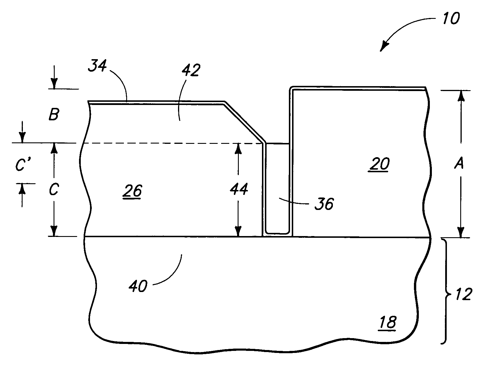
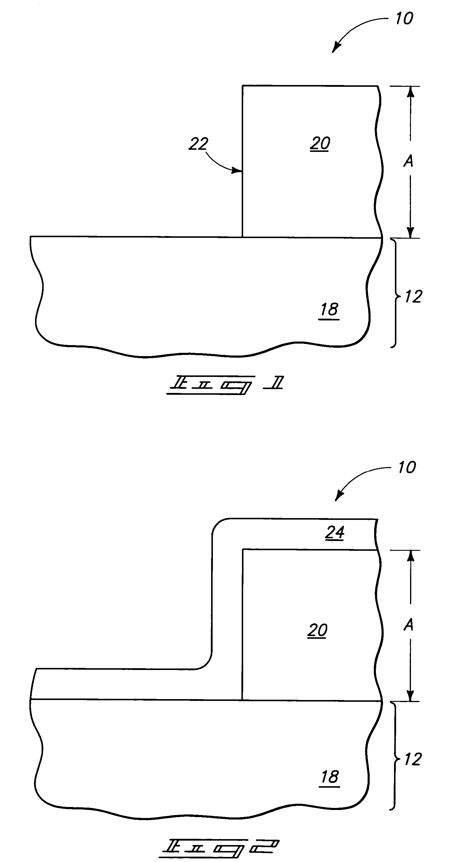
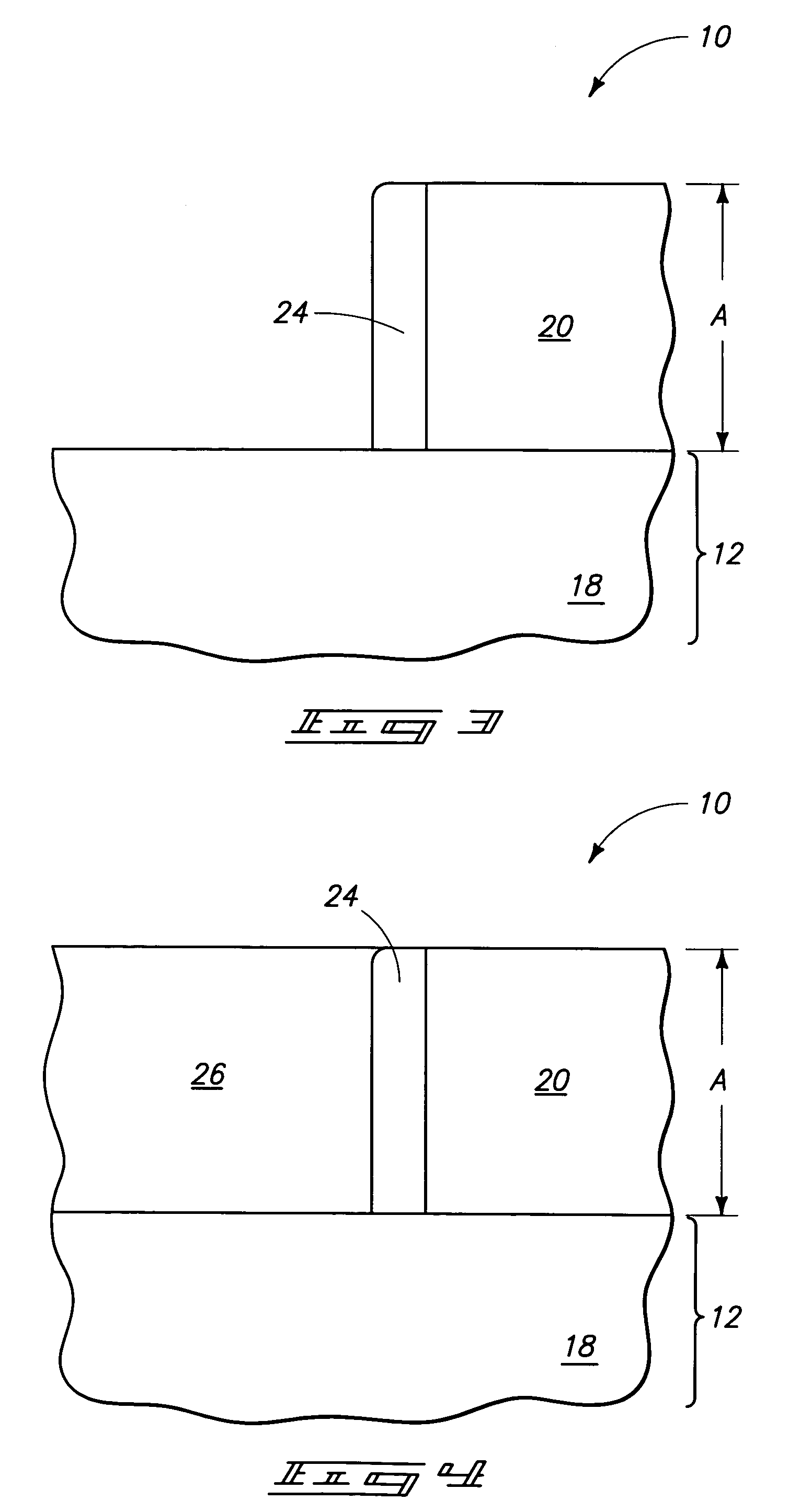
[0027]An exemplary embodiment of a method of forming a field effect transistor is initially described with reference to FIGS. 1-8. FIG. 1 depicts a substrate fragment 10 comprising a semiconductor substrate 12. In the context of this document, the term “semiconductor substrate” or “semiconductive substrate” is defined to mean any construction comprising semiconductive material, including, but not limited to, bulk semiconductive materials such as a semiconductive wafer (either alone or in assemblies comprising other materials thereon), and semiconductive material layers (either alone or in assemblies comprising other materials). The term “substrate” refers to any supporting structure, including, but not limited to, the semiconductive substrates described above. Further in the context of th...


PUM


Abstract

A mass of material is formed over a semiconductor substrate. Semiconductive material is formed laterally proximate the mass of material. A space is provided laterally between the mass of material and the semiconductive material. The space comprises an outermost portion and a portion immediately adjacent thereto. The outermost portion has a maximum lateral width which is greater than that of the adjacent portion. Gate dielectric material and conductive gate material are formed within the space. The gate dielectric material and the conductive gate material in combination fill the adjacent portion of the space but do not fill the outermost portion of the space. At least the conductive gate material is etched from at least a majority of the outermost portion of the space. Source / drain regions are formed operatively proximate the conductive gate material and the semiconductive material is used as a channel region of the field effect transistor.

Description

TECHNICAL FIELD[0001]This invention relates to methods of forming field effect transistors.BACKGROUND OF THE INVENTION[0002]A continuing goal in integrated circuitry design is to make ever denser, and therefore smaller, circuit devices. This results in thinner layers and smaller geometries. Further, new deposition techniques and materials are constantly being developed to enable circuit devices to be made smaller than the previous generations. Additionally, circuit designs sometimes fabricate the devices to be substantially horizontally oriented relative to the underlying substrate, and sometimes substantially vertically oriented.[0003]One common circuitry device is a field effect transistor. Such includes a pair of conductive source / drain regions having a semiconductive channel region received therebetween. A conductive gate is received proximate the channel region, with a gate dielectric layer being received between the gate and the channel region. Application of a suitable voltag...

Claims


Application Information

Patent Timeline
Patent Type & Authority Patents(United States)
IPC IPC(8): H01L21/336
CPCH01L29/66666H01L29/7827
Inventor SANDHU, GURTEJ S.MANNING, H. MONTGOMERYBASCERI, CEM
Owner MICRON TECH INC
Features
  • Generate Ideas
  • Intellectual Property
  • Life Sciences
  • Materials
  • Tech Scout
  • Unparalleled Data Quality
  • Higher Quality Content
  • 60% Fewer Hallucinations
Learn More