Wafer-level package for integrated circuits

a technology of integrated circuits and packages, applied in the field of integrated circuit packages, can solve the problems of time-consuming and expensive packaging of individual dies, and achieve the effect of convenient attachmen

Active Publication Date: 2007-08-28
MEMSIC
View PDF11 Cites 26 Cited by
  • Summary
  • Abstract
  • Description
  • Claims
  • Application Information

AI Technical Summary

Benefits of technology

[0008]Thus, all the die on the IC wafer can be packaged in a single operation, and then the packaged die are singulated, significantly reducing the time and cost to package the die. These and other features, advantages, aspects and embodiments of the present invention will become more apparent to those skilled in the art from the Detailed Description of the Invention that follows.

Problems solved by technology

However, after the die are singulated, packaging the individual die (the “back-end” process of IC fabrication) is time consuming and expensive, because each die must be packaged individually (i.e., serially).

Method used


Image

  • Wafer-level package for integrated circuits
  • Wafer-level package for integrated circuits
  • Wafer-level package for integrated circuits

Examples


Embodiment Construction

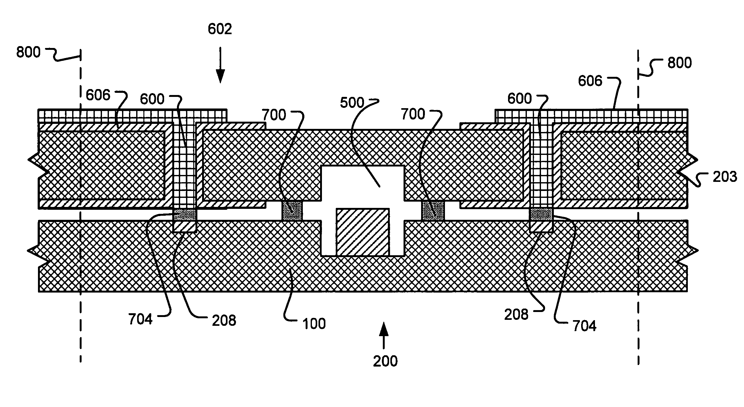
[0017]Embodiments of the present invention include wafer-level packages for integrated circuits (ICs), as well as methods for fabricating wafer-level packaged ICs and their components. A wafer-level packaged IC is made by attaching a semiconductor cap wafer to an IC wafer before cutting the IC wafer, i.e. before singulating the plurality of die on the IC wafer. The cap wafer is overlaid over some or all of the die on the IC wafer, then the cap wafer is mechanically attached to the IC wafer. For example, the wafers can be attached to each other by solder at various counterfacing locations on the cap wafer and on the IC wafer in the vicinity of each die. Each die is sealed between the cap wafer and the IC wafer, such as to prevent infiltration of moisture. The seal can be provided by the mechanical attachment between the cap wafer and the IC wafer, or the seal and the mechanical attachment can be provided by separate elements.

[0018]The IC wafer contains at least one electrical contact...


PUM


Abstract

A wafer-level packaged IC is made by attaching a cap wafer to the top of an IC wafer before cutting the IC wafer, i.e. before singulating the plurality of die on the IC wafer. The cap wafer is mechanically attached and electrically connected to the IC wafer, then the die are singulated. Electrically conductive paths extend through the cap wafer, between wafer contact pads on the top surface of the cap and electrical contact points on the IC wafer. Optionally, the cap wafer contains one or more die. The IC wafer can be fabricated according to a different technology than the cap wafer, thereby forming a hybrid wafer-level package. Optionally, additional “upper-level” cap wafers (with or without die) can be stacked to form a “multi-story” IC.

Description

CROSS REFERENCE TO RELATED APPLICATIONS[0001](Not applicable)STATEMENT REGARDING FEDERALLY SPONSORED RESEARCH OR DEVELOPMENT[0002](Not applicable)BACKGROUND OF THE INVENTION[0003]The present invention relates to integrated circuit packages and, more particularly, to wafer-level packages for integrated circuits. Integrated circuits (ICs) are manufactured as wafers, each wafer containing many individual circuits (die). After fabrication, a wafer is cut (“singulated”) into individual die. Each die is then encapsulated in a plastic or ceramic package or is attached to a ceramic cap.[0004]Each die includes several electrical contact pads. During packaging, each of these contact pads is connected to a respective lead or another external structure. In one common practice, a bonding wire is welded between each contact pad and a respective lead. The leads or other structures are used to electrically connect a completed IC to a circuit board or the like, such as by soldering. These solder con...

Claims


Application Information

Patent Timeline
Patent Type & Authority Patents(United States)
IPC IPC(8): G01R31/02G01R31/26
CPCH01L21/50H01L23/10H01L25/0657H01L21/76898H01L23/481H01L2224/16H01L2225/06572H01L2225/06582H01L2924/01079H01L24/03H01L24/05H01L2224/0554H01L2224/0557H01L2224/05571H01L2224/05573H01L2924/00014H01L2924/1627H01L2224/05599H01L2224/0555H01L2224/0556
Inventor ZHAO, YANG
Owner MEMSIC
Why Eureka
Try Eureka