Method for optimising transistor performance in integrated circuits

a technology of integrated circuits and transistors, applied in the field of integrated circuits, can solve the problems of 10% or more variation of output performance, physical properties of asic, stress occurring in materials, etc., and achieve the effect of optimizing transistor performan

Active Publication Date: 2007-09-04
ICERA INC
View PDF14 Cites 110 Cited by
  • Summary
  • Abstract
  • Description
  • Claims
  • Application Information

AI Technical Summary

Problems solved by technology

However, as a result of this technology scaling, additional problems have surfaced concerning the physical properties of the ASIC.
Such a problem includes stress occurring in materials near an interface of different materials with different crystallographic structures or thermal expansion coefficients.
For example, in the NMOS and PMOS devices, such as field effect transistors (FET), the impact of the stress may be severe and result in 10% or more variation of output performance.

Method used


Image

  • Method for optimising transistor performance in integrated circuits
  • Method for optimising transistor performance in integrated circuits
  • Method for optimising transistor performance in integrated circuits

Examples


Embodiment Construction

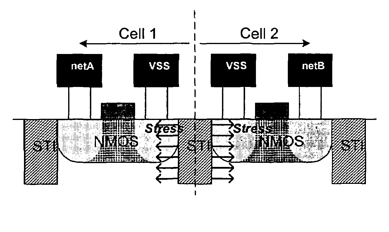
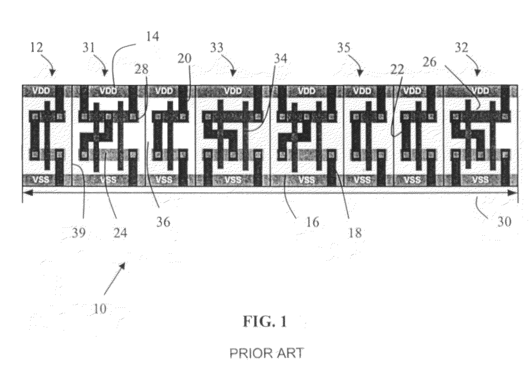
[0015]With reference to FIG. 1, a physical layout of a row of logic cells is shown arranged in a conventional manner. A conventional cell includes non-active areas 36, for example STI regions, surrounding active areas or regions 24,26,34 within each cell. There may be STI regions within a cell, especially when the cell has more than two stages, however the STI regions 36 also act to divide and isolate active areas from one another and form cell boundaries between the cells at the block level. The STI regions forming cell boundaries straddle the border of two adjacent cells. The active areas include the diffusion 24,26 and gate areas 34. The supply nets 20,18 are supply connections between positive-channel 26 and negative-channel diffusion 24 and respective power rails 14,16 (VDD,VSS). The supply nets may be configured along a boundary or an edge 39 of the cell. A boundary or edge 39 of the cell is defined by a continuous STI region 36 that straddles across two adjacent cells, at the...


PUM


Abstract

A method (300) for optimising transistor performance in semiconductor integrated circuits built from standard cells (12), or custom transistor level layout, is disclosed. An active area of NMOS diffusion is extended with a joining area (102) between two adjacent cells (112) having the same net on diffusion at the adjacent edges of each cell. The diffusion area is extended to limit the occurrence of active and nonactive interface to minimise lattice strain effects and improve transistor performance.

Description

FIELD OF THE INVENTION[0001]This invention relates generally to integrated circuits, and more particularly to methods for optimising performance of logic cells within a standard cell library for large scale integration of semiconductor integrated circuits.BACKGROUND[0002]Conventional standard cell libraries in semiconductor integrated circuits (IC) primarily contain a logic cell layout based in a metal oxide semiconductor (MOS) environment, in particular a complimentary metal oxide semiconductor (CMOS) environment. A standard cell is a pre-designed layout of transistors or non-specific collection of logic gates that are typically designed with computer assisted design (CAD) applications. The cells are usually interconnected or wired together in a particular manner with means of a placement and routing tool to perform a specific type of logical operation in an application specific IC (ASIC). A conventional ASIC layout is typically defined by an array of logic cells arranged in adjace...

Claims


Application Information

Patent Timeline
Patent Type & Authority Patents(United States)
IPC IPC(8): G06F17/50
CPCH01L27/0207H01L27/11807
Inventor HUGHES, PETER WILLIAMMORTON, SHANNON VANCEMONK, TREVOR KENNETH
Owner ICERA INC
Why Eureka
Try Eureka