Spring-based probe pin that allows kelvin testing

a probe pin and spring technology, applied in the field of probe pins, can solve the problems of two conventional spring-based probe pins not being able to cantilever pins can significantly damage the solder bumps, and cantilever pins cannot be used in kelvin testing

Active Publication Date: 2007-09-18
NAT SEMICON CORP
View PDF17 Cites 27 Cited by
  • Summary
  • Abstract
  • Description
  • Claims
  • Application Information

AI Technical Summary

Problems solved by technology

One significant disadvantage of probe pin 216A, and pogo pins in general, is that conventional spring-based probe pins can not be used in a kelvin test.
Since spring-based probe pins are axially aligned with the solder bumps to contact the apexes of the solder bumps, it is not possible for two conventional spring-based probe pins to make an electrical connection with a single solder bump without severely damaging the solder bump.
One disadvantage of cantilever pins, however, is that the cantilever pins can significantly damage the solder bumps when the cantilever pins and solder bumps are brought into contact.
Since cantilever pins approach the solder bumps from the side, it is not uncommon for a cantilever pin to first make contact with a solder bump, and then undesirably scratch across the surface of the solder bump as the full contact force is applied to make the electrical connection.

Method used


Image

  • Spring-based probe pin that allows kelvin testing
  • Spring-based probe pin that allows kelvin testing
  • Spring-based probe pin that allows kelvin testing

Examples


Embodiment Construction

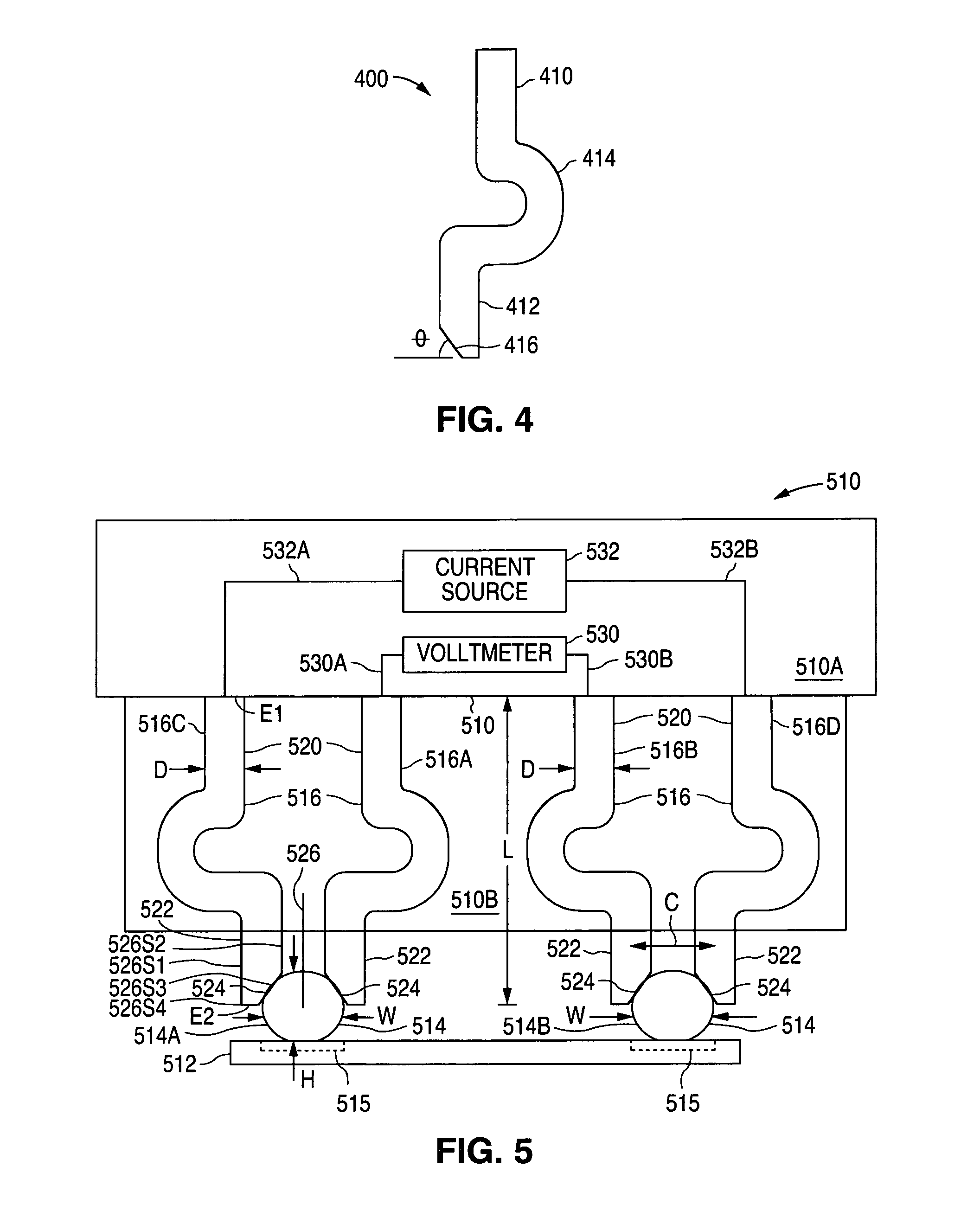
[0025]FIG. 4 shows a cross-sectional diagram that illustrates an example of a spring-based probe pin 400 in accordance with the present invention. As described in greater detail below, by offsetting and tapering the lower end section of a spring-based probe pin, multiple pins can be connected to a single solder bump, thereby allowing a kelvin test to be performed.

[0026]As shown in the FIG. 4 example, probe pin 400 is implemented as a single metal element that has a top end section 410, a bottom end section 412, and a C-shaped section 414 that connects sections 410 and 412 together. In addition, in accordance with the present invention, bottom end section 412 has a tapered surface 416. Tapered surface 416 is flat, and has an angle θ, such as 45°, which is selected to minimize contact damage. Other angles, as well as a curved surface that generally matches the surface of a solder bump, can also be used to form tapered surface 416.

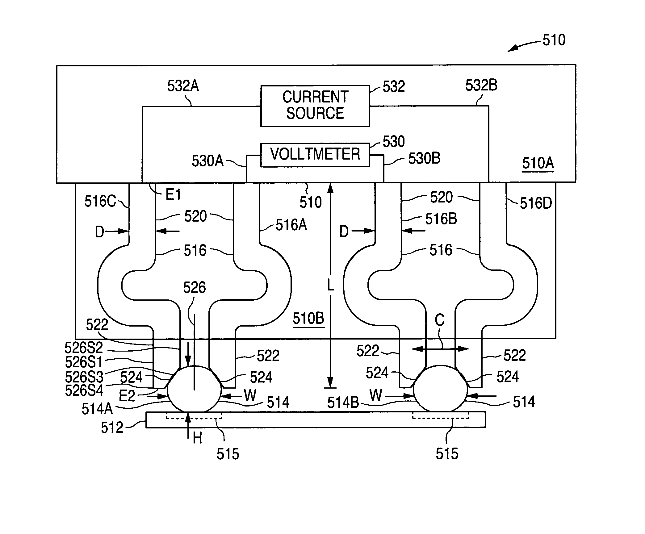
[0027]FIG. 5 shows a cross-sectional diagram that illus...


PUM


Abstract

The voltage at a node of an integrated circuit can be measured or controlled using a two-wire kelvin contact with spring-based probe pins by offsetting and tapering the lower end section of the spring-based probe pin. As a result, multiple spring-based probe pins can be connected to a single contact bump, such as a solder bump.

Description

BACKGROUND OF THE INVENTION[0001]1. Field of the Invention[0002]The present invention relates to probe pins and, more particularly, to a spring-based probe pin that allows kelvin testing.[0003]2. Description of the Related Art[0004]A bumped die package is a package that eliminates the need for wire bonding and molding. With a bumped die process, solder bumps are mounted to the bond pads of a wafer, which is then diced to form a large number of individual die. Once diced, an individual die is ready to be used by a customer.[0005]Final electrical testing is performed using a test and evaluation circuit that includes a number of probe pins. In operation, the probe pins are brought into electrical contact with the solder bumps. Voltages and currents are then applied to the solder bumps via the probe pins so that the proper operation of the circuits can be verified.[0006]In current-generation test and evaluation circuits, the probe pins are commonly implemented as pogo pins or cantilever...

Claims


Application Information

Patent Timeline
Patent Type & Authority Patents(United States)
IPC IPC(8): G01R31/02G01R27/08G01R31/28
CPCG01R1/06738G01R1/07314G01R27/14
Inventor TANG, TZE KANGCHONG, SEK HOIGAN, CHIN CHAITAN, HAI CHING
Owner NAT SEMICON CORP
Why Eureka
Try Eureka