Electro-optical integrated transmitter chip for arbitrary quadrature modulation of optical signals

a transmitter chip and optical signal technology, applied in the field of optical signal arbitrary quadrature modulation devices, can solve the problems of reduced performance and increased cost, no fully planar integrated solution for the device, and inability to implemen

Inactive Publication Date: 2007-09-18
CELIGHT
View PDF19 Cites 78 Cited by
  • Summary
  • Abstract
  • Description
  • Claims
  • Application Information

AI Technical Summary

Problems solved by technology

This practice reduces performance and increases cost.
Such communication schemes were abandoned in the late 1980's and are still not implemented due to their complexity and

Method used


Image

  • Electro-optical integrated transmitter chip for arbitrary quadrature modulation of optical signals
  • Electro-optical integrated transmitter chip for arbitrary quadrature modulation of optical signals
  • Electro-optical integrated transmitter chip for arbitrary quadrature modulation of optical signals

Examples


Embodiment Construction

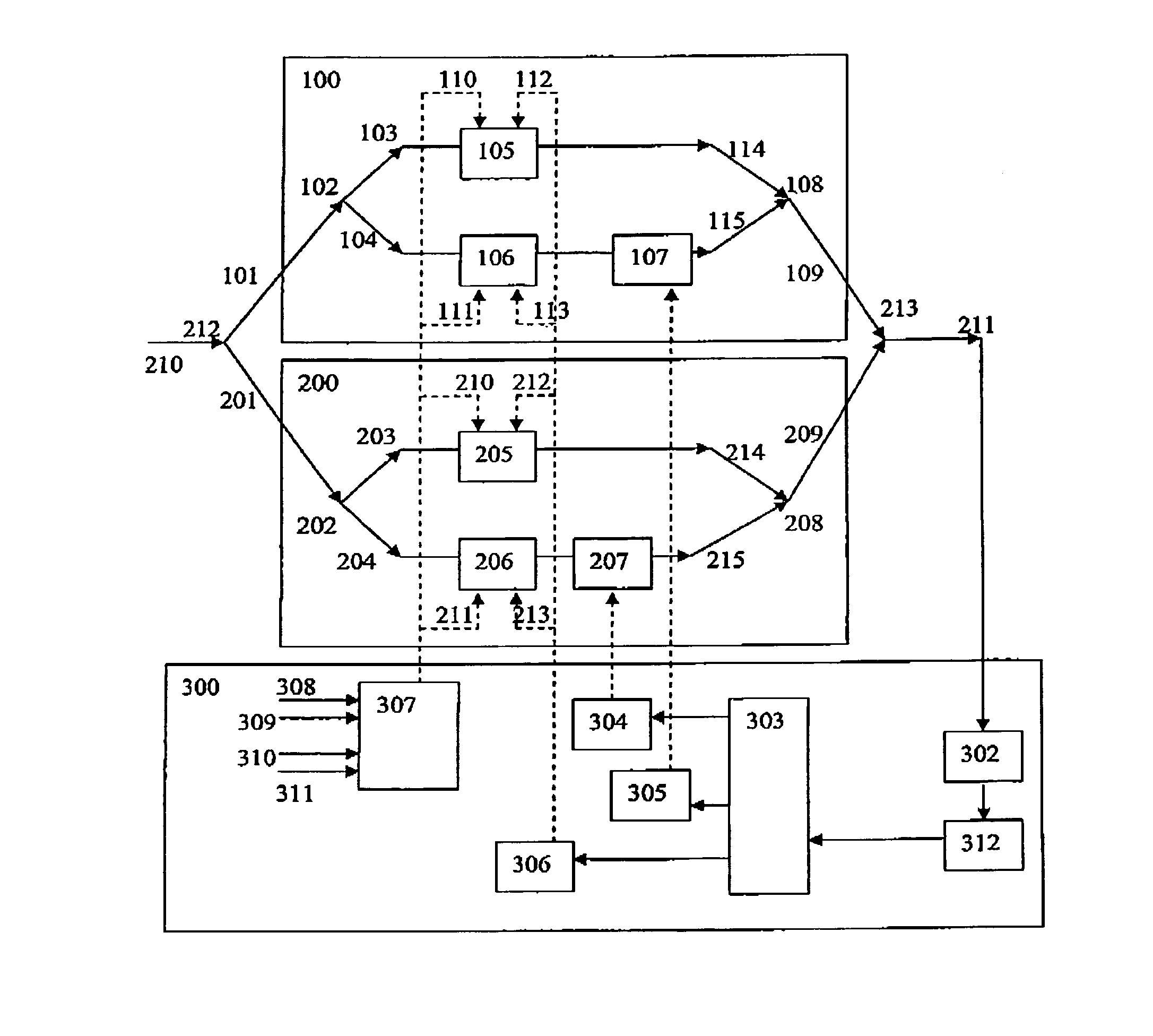
[0041]In one embodiment of the present invention, an optical device is provided that includes, a first Mach-Zehnder modulator that produces a first output, and a second Mach-Zehnder modulator which produces a second output. The first and second Mach-Zehnder modulators are coupled to an input splitter. A combiner combines the first and second outputs from first and second Mach-Zehnder modulators. A phase shifter is coupled to the first and second Mach-Zehnder modulators. The first Mach-Zehnder modulator, second Mach-Zehnder modulator, input splitter, combiner and the phase shifter are each formed as part of a single chip made of electro-optical material.

[0042]In various embodiments, the optical device of the present invention is an integrated optical device that is formed on a single chip, single piece of crystal including but not limited to a monolithic piece of a crystal wafer, that can be made of an electrooptical crystal including but not limited to LiNBO3. In one embodiment, dif...


PUM


Abstract

An optical device includes, a first Mach-Zehnder modulator that produces a first output, and a second Mach-Zehnder modulator which produces a second output. A splitter couples the first and second Mach-Zehnder modulators. A combiner combines the first and second outputs. A phase shifter is coupled to the first and second Mach-Zehnder modulators. The first Mach-Zehnder modulator, second Mach-Zehnder modulator, splitter, combiner and the phase shifter are each formed as part of a single chip made of electro-optical material. Such two similar optical device integrated together with polarization combiner provide a two-polarization performance.

Description

CROSS-REFERENCE TO RELATED APPLICATIONS[0001]The present invention claims the benefit of U.S. Ser. No. 60 / 392,938, filed Jul. 2, 2002 and is also a continuation-in part of U.S. Ser. No. 09 / 962,243, filed Sep. 26, 2001, now U.S. Pat. No. 7,167,651, U.S. Ser. No. 09 / 962,339, filed Sep. 26, 2001, now U.S. Pat. No. 7,110,677, and U.S. Ser. No. 10 / 084,057, filed February 28, 2002, all of which applications are fully incorporated herein by reference.BACKGROUND OF THE INVENTION[0002]1. Field of the Invention[0003]This invention relates generally to electro-optical modulation devices and their methods and use, and more particularly to electro-optical modulation devices formed on a single chip, and their methods of use.[0004]2. Description of the Related Art[0005]Lasers are widely used today in fiber and free space segments for high data rate communication links, remote sensing applications (LIDAR) and more. In these applications the light signal is modulated, usually using electro-optical m...

Claims


Application Information

Patent Timeline
IPC IPC(8): G02F1/035G02B6/26G02B6/42G02F1/225H04B10/148H04B10/155H04B10/18H04J14/00H04J14/02H04J14/08H04L7/00
CPCG02F1/225H04B10/2543H04B10/505H04B10/5053H04B10/5057H04B10/50577H04B10/508H04B10/532H04B10/541H04B10/5561H04B10/60H04J14/005H04J14/02H04J14/08H04L7/0075G02F2203/06
Inventor KAPLAN, ARKADYACHIAM, YAAKOVGREENBLATT, ARTHURSHPANTZER, ISAACCHO, PAK SHINGTSEYTLIN, MICHAELSALAMON, AVIV
Owner CELIGHT
Why Eureka
Try Eureka