Optical transmitter

a technology of optical transmitters and optical beams, applied in the field of optical transmitters, can solve the problems of difficult to increase the coupling efficiency, difficult to couple light beams, and failure to ensure in the direction of the thickness of the optical transmitter, so as to reduce the number of components and simplify the production process. , the effect of increasing the coupling efficiency

Inactive Publication Date: 2007-10-16
SHARP KK
View PDF13 Cites 23 Cited by
  • Summary
  • Abstract
  • Description
  • Claims
  • Application Information

AI Technical Summary

Benefits of technology

[0028]The present invention has been made under these circumstances, and it is an object of the present invention to provide an optical transmitter good in heat dissipation which has high coupling efficiency. The optical transmitter can also be miniaturized and manufactured at a low cost, and can be used and stored over a wide temperature range.
[0030]In the first optical transmitter according to the present invention, the substrate has the through hole. The through hole has the inner wall. The through hole has the inside diameter increasing from the rear surface side of the substrate toward the front surface side thereof. Thus, of light beams radiated from the light-emitting portion, a light beam having a wide radiation angle can be reflected from the inner wall of the through hole toward the front surface of the substrate. Accordingly, the light beam having a wide radiation angle, of the light beams radiated from the light-emitting element, can be also effectively utilized for optical coupling into an optical fiber or the like, increasing the coupling efficiency.
[0031]The light-emitting element is disposed on the rear surface of the substrate so that the light-emitting portion is exposed within the through hole. Thus, the light-emitting portion of the light-emitting element is close to the inner wall of the through hole. Accordingly, it is possible to reduce to a minimum the depth of the through hole involved in reflection of a light beam having a wide radiation angle toward the front surface of the substrate. Consequently, miniaturization of the optical transmitter can be achieved.
[0032]The through hole formed in the substrate serves as a guide for light beams radiated from the light-emitting element. Thus, the substrate originally for use as a wiring component can also be utilized as an optical component. Accordingly, the number of components can be reduced and the production process can be simplified. Consequently, cost reduction of the optical transmitter can be achieved.
[0033]The light-emitting element is disposed so that the light-emitting portion is exposed within the through hole. Thus, the light-emitting portion as a heat-generating source is close to the substrate as a heat-dissipating medium. Accordingly, heat dissipation of the light-emitting element is improved.

Problems solved by technology

However, there is a problem with this optical transmitter that it is difficult to couple light beams radiated form the LED 103 into the optical fiber 102 with high efficiency.
However, bringing the lens 104 closer to the LED 103 causes the failure to ensure in a direction of the thickness of the optical transmitter a space required for wire-bonding of an electrode of the LED 103 to the lead frame.
However, in an optical transmitter using a concave mirror, it is difficult to increase the coupling efficiency while achieving miniaturization and cost reduction of the optical transmitter.
If the inside diameter of the concave mirror 108 on a side at which radiated light beams are raised, i.e., on the upper edge side, is as large as about φ 2 mm, there is a risk that, when a lens with a short focal length is used to collect light beams, the light beams may not be able to be coupled into the optical fiber because an NA incident to the optical fiber becomes so large that the light beams cannot be coupled into the optical fiber.
On the other hand, when using a lens with a long focal length in order to take an advantage of a small incident NA, it is difficult to miniaturize the optical transmitter inclusive of the optical fiber.
Further, a space needs to be provided at a portion of the concave mirror 108 for wire-bonding the electrode of the LED 103, which complicates the production process and widens a variation in transmission efficiency and thus a variation in the quantity of light coupled into the optical fiber.
Also, the substrate 205 needs to have therein the concave mirror 108, which results in a high cost.
As has been explained above, in an optical transmitter using a concave mirror, after all, it is difficult to increase the coupling efficiency while achieving miniaturization and cost reduction of the optical transmitter.
These optical transmitters are problematic in that the number of components is increased to result in upsizing and a rise in the cost of the optical transmitters.
However, only forming the opening through the lead frame for a light beam to pass through the opening does not make it possible to guide a light beam with a wide radiation angle to the lens at an effective angle.
Therefore, it is eventually difficult to utilize a light beam with a wide radiation angle.
If the optical transmitter is poor in heat dissipation, the temperature of a light-emitting element chip itself rises.
Therefore, the magnitude of an electric current allowed to pass through the light-emitting element is limited, and the environment in which optical transmitters can be used is limited to make it impossible to use them in environments where the temperature is high such as motor vehicles and production facilities.
However, with this method there is a problem in that the thermal resistance of the LED chip itself cannot be reduced and that a high cost and upsized optical transmitters are resulted.
For this reason, there is a problem in that, in environments where wide temperature variations (e.g., from −40° C. to 110° C.) are encountered as expected in vehicle-installed devices and the like, a great thermal stress is applied onto the light-emitting surface of the LED 103 to make the light emission state unstable or make the LED 103 broken, or a bonding wire is ruptured due to a difference in linear expansivity between the bonding wire and the epoxy resin.
Thus, it is difficult to gain a high reliability.

Method used


Image

  • Optical transmitter
  • Optical transmitter
  • Optical transmitter

Examples


embodiment 1

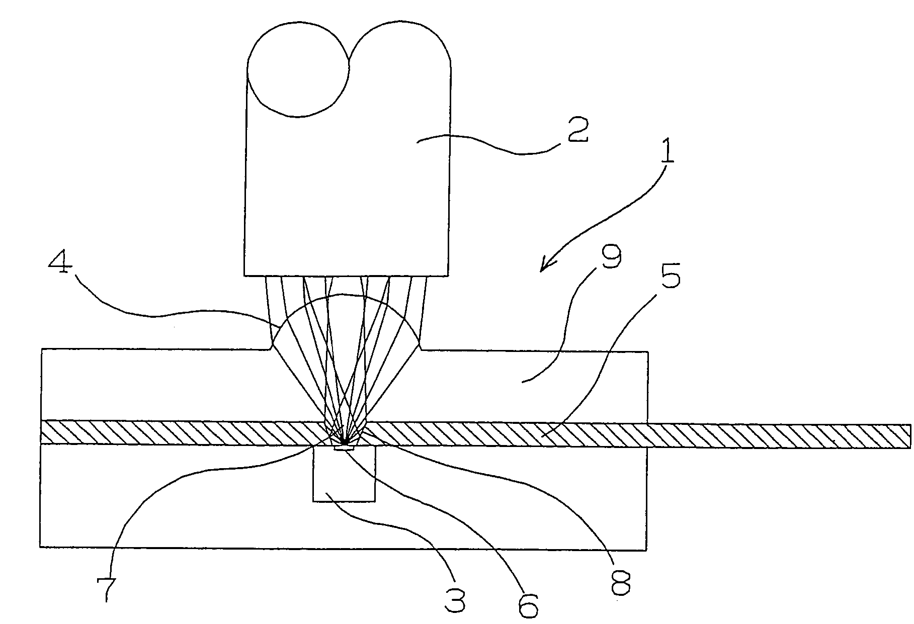
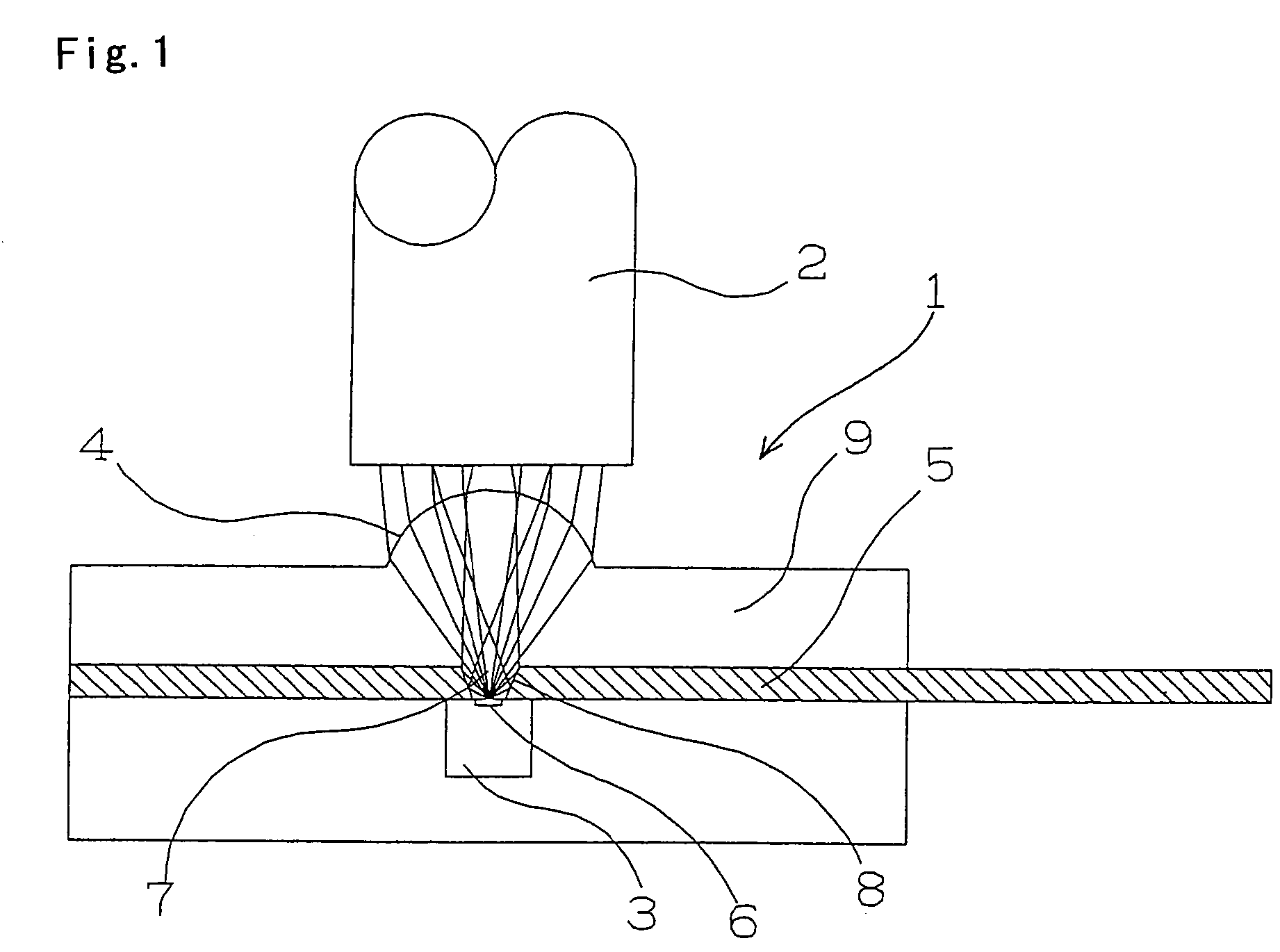
[0111]FIG. 1 is an explanatory view showing a schematic construction of an optical transmitter according to Embodiment 1 of the present invention.

[0112]The optical transmitter 1 comprises a light-emitting element 3, a lens 4 and a lead frame (substrate) 5 disposed on the light-emitting element 3.

[0113]The lead frame 5 has a through hole 7 formed in a position facing a light-emitting surface (light-emitting portion) 6 of the light-emitting element 3. The through hole 7 is tapered so that its inside diameter gradually increases from a rear surface side, on which the light-emitting element 3 is disposed, toward a front surface side. The tapered through hole 7 has an inner wall called a taper mirror 8.

[0114]Of light beams radiated from the light-emitting element 3, a light beam having a narrow radiation angle passes through the through hole 7 and enters the lens 4 to be refracted and coupled into an optical fiber 2. A light beam having a wide radiation angle of the light beams radiated ...

embodiment 2

[0180]A modification of the above optical transmitter according to Embodiment 1 is given as an optical transmitter according to Embodiment 2 and explained referring to FIG. 14. FIG. 14 is an explanatory view showing a schematic structure of the optical transmitter according to Embodiment 2.

[0181]As shown in FIG. 14, in the optical transmitter 21 according to Embodiment 2, the lens 4 is not formed of the mold resin (encapsulating resin member) 9. The mold resin 9 covers only the rear surface side of the lead frame 5 on which the light-emitting element 3 is disposed. The light-emitting element 3 and a driver IC 19 are encapsulated in the mold resin 9 and protected from outside air. The light-emitting element 3 and the driver IC 19 are electrically connected together with a bonding wire 33 (though in the reality there are a plurality of bonding wires 33, omission is made in the figure).

[0182]The lens 4 can be a ball lens made of a glass, an acrylic resin or the like. The ball lens as t...

embodiment 3

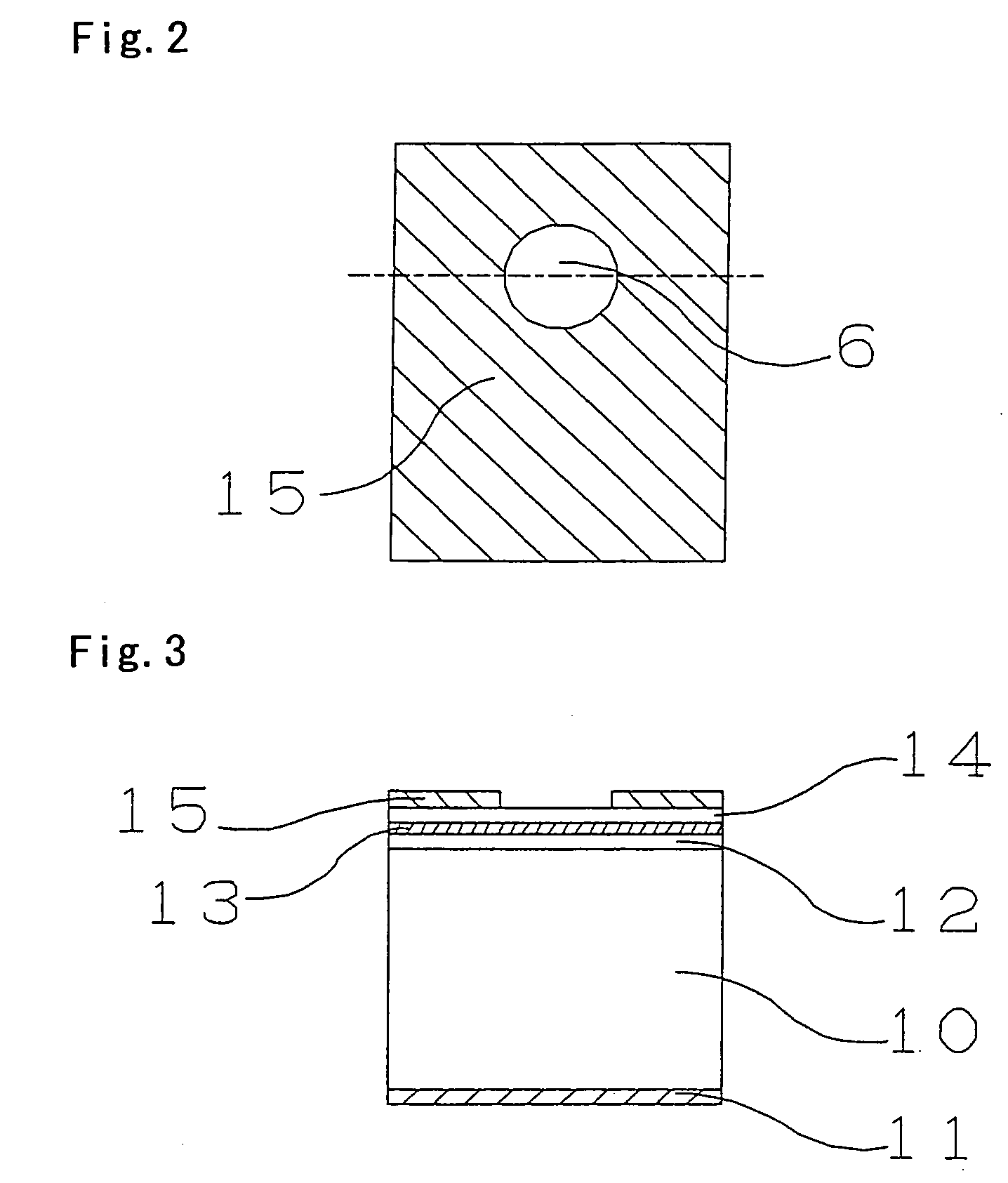
[0187]Another modification of the above optical transmitter according to Embodiment 1 is given as an optical transmitter according to Embodiment 3 and explained referring to FIG. 15. FIG. 15 is an enlarged view of an essential part of the optical transmitter according to Embodiment 3.

[0188]As shown in FIG. 15, in the optical transmitter 31 according to Embodiment 3, the through hole 7 is of the shape shown in FIGS. 10 and 11.

[0189]A light beam emitted from the light-emitting element is reflected from the taper mirror portion 8, without being applied onto the inner wall of the enlarged hole portion 17, so that the optical path of the light beam is changed.

[0190]As aforementioned, this constitution allows the lead frame 5 to have an increased thickness so that heat dissipation is improved, and further that the effect of the mold resin (light-transmissive resin member) 9 or the adhesive (transparent resin) 16 easily flowing into the through hole 7 can be obtained.

[0191]Also, the light-...


PUM


Abstract

The present invention provides an optical transmitter for transmitting an optical signal using an optical fiber as a transmission medium. The optical transmitter comprises: a substrate having a through hole; and a light-emitting element disposed on a rear surface of the substrate and having a light-emitting portion. The through hole has an inner wall. The through hole has an inside diameter increasing from a rear surface side of the substrate toward a front surface side thereof. The light-emitting element is disposed so that the light-emitting portion is exposed within the through hole. The light-emitting portion radiates light beams toward a front surface of the substrate. The through hole is such that part of the light beams goes out the through hole without being reflected, and that the other light beams go out the through hole after being reflected from the inner wall thereof. It is possible to increase the coupling efficiency of the optical transmitter by effectively utilizing a light beam light having a wide radiation angle, and improve heat dissipation thereof, while achieving miniaturization and cost reduction of the optical transmitter.

Description

TECHNICAL FIELD[0001]The present invention relates to an optical transmitter. More particularly, the present invention relates to an optical transmitter for transmitting an optical signal using an optical fiber as a transmission medium.BACKGROUND ART[0002]There have been known optical transmitters using a light-emitting diode as a light source and a multimode optical-fiber as a transmission medium in domestic communications, in communications inside of motor vehicles and the like using LAN (Local Area Network). As prior arts associated with the present invention, the following are known.[0003](1) A photosemiconductor device characterized by comprising: a pair of conductive leads arranged facing each other; a metal container having a reflecting surface and disposed at a distal end of one of the conductive leads; a photosemiconductor element disposed on the reflecting surface of the metal container, one electrode of the photosemiconductor element being connected to one of the conducti...

Claims


Application Information

Patent Timeline
Patent Type & Authority Patents(United States)
IPC IPC(8): G02B6/36H01L33/00H01L33/58H01L33/60H01L33/62
CPCH01L33/60H01L33/62H01L33/58H01L2924/0002H01L2924/00
Inventor FUJITA, HIDEAKI
Owner SHARP KK
Why Eureka
Try Eureka