Semiconductor laser and optical module

a semiconductor laser and optical module technology, applied in semiconductor lasers, optical elements, instruments, etc., can solve the problems of reducing the coupling efficiency of laser beams, unable to obtain a desirable circular narrow emitted beam divergence from the viewpoint of reducing the optical coupling efficiency of horizontal cavity surface emitting lasers, and reducing the fabrication cost of optical modules or optical transceivers. , to achieve the effect of improving the optical coupling efficiency of optical modules, facilitating mounting processes,

Active Publication Date: 2009-03-10
LUMENTUM JAPAN INC
View PDF6 Cites 7 Cited by
  • Summary
  • Abstract
  • Description
  • Claims
  • Application Information

AI Technical Summary

Benefits of technology

[0009]A first object of the present invention is to provide a horizontal cavity surface emitting semiconductor laser that emits a circular narrow-divergence emitted beam and is high in the coupling efficiency between the fiber and the optical waveguide. Also, a second object of the present invention is to provide an optical module that is high in the optical coupling efficiency. Further, a third object of the present invention is to provide an optical transceiver that is high in the optical coupling efficiency.
[0015]According to the present invention, it is possible to realize the horizontal cavity surface emitting laser that emits the circular narrow-divergence emitted beam. For that reason, it is possible to improve the optical coupling efficiency of the optical module using the present laser device or the optical transceiver. Also, since the high-precision alignment is not required at the time of mounting the laser by using the laser device of the present invention, the mounting process is facilitated, and it is possible to realize a remarkable reduction in the fabrication cost of the optical module or the optical transceiver.

Problems solved by technology

The conventional horizontal cavity surface emitting laser suffers from such a problem that the laser emitted beam is oval.
However, in the case where the laser beam that is emitted from the semiconductor laser is coupled to a fiber or the like, it is desirable that the beam contour of the laser beam is circular, and the narrow beam divergence is provided in order to reduce the coupling efficiency of the laser beam.
As described above, in the conventional technique, it is impossible to obtain a desirable circular narrow emitted beam divergence from the viewpoint of the reduction in the optical coupling efficiency in the horizontal cavity surface emitting laser.

Method used


Image

  • Semiconductor laser and optical module
  • Semiconductor laser and optical module
  • Semiconductor laser and optical module

Examples


first embodiment

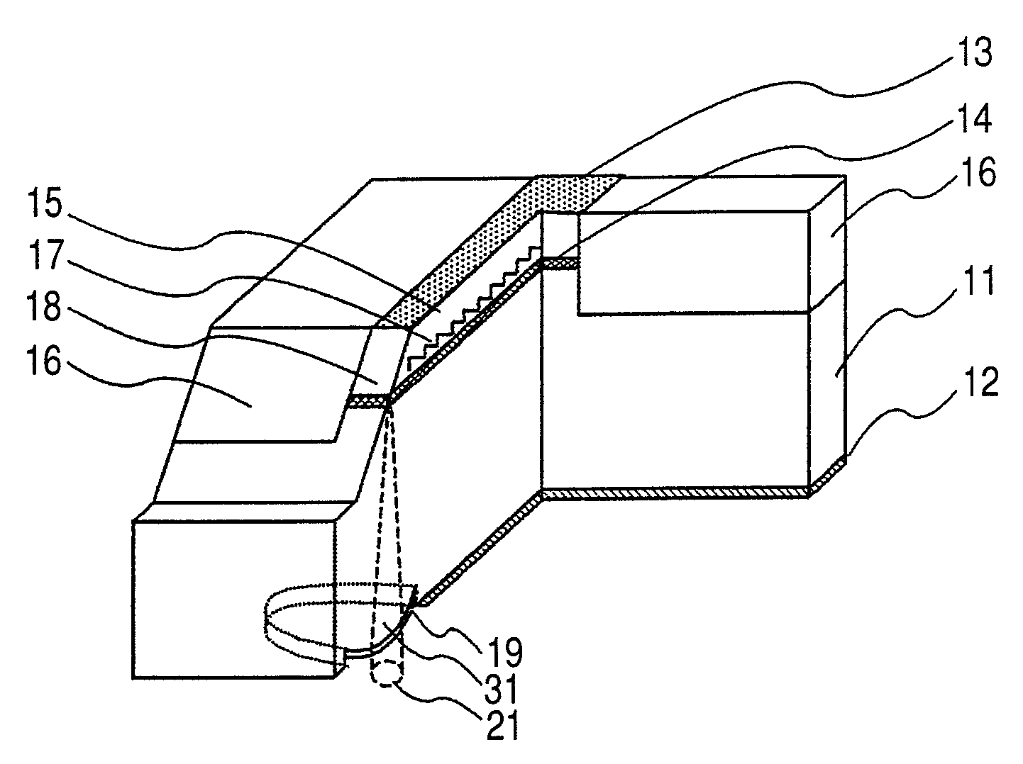
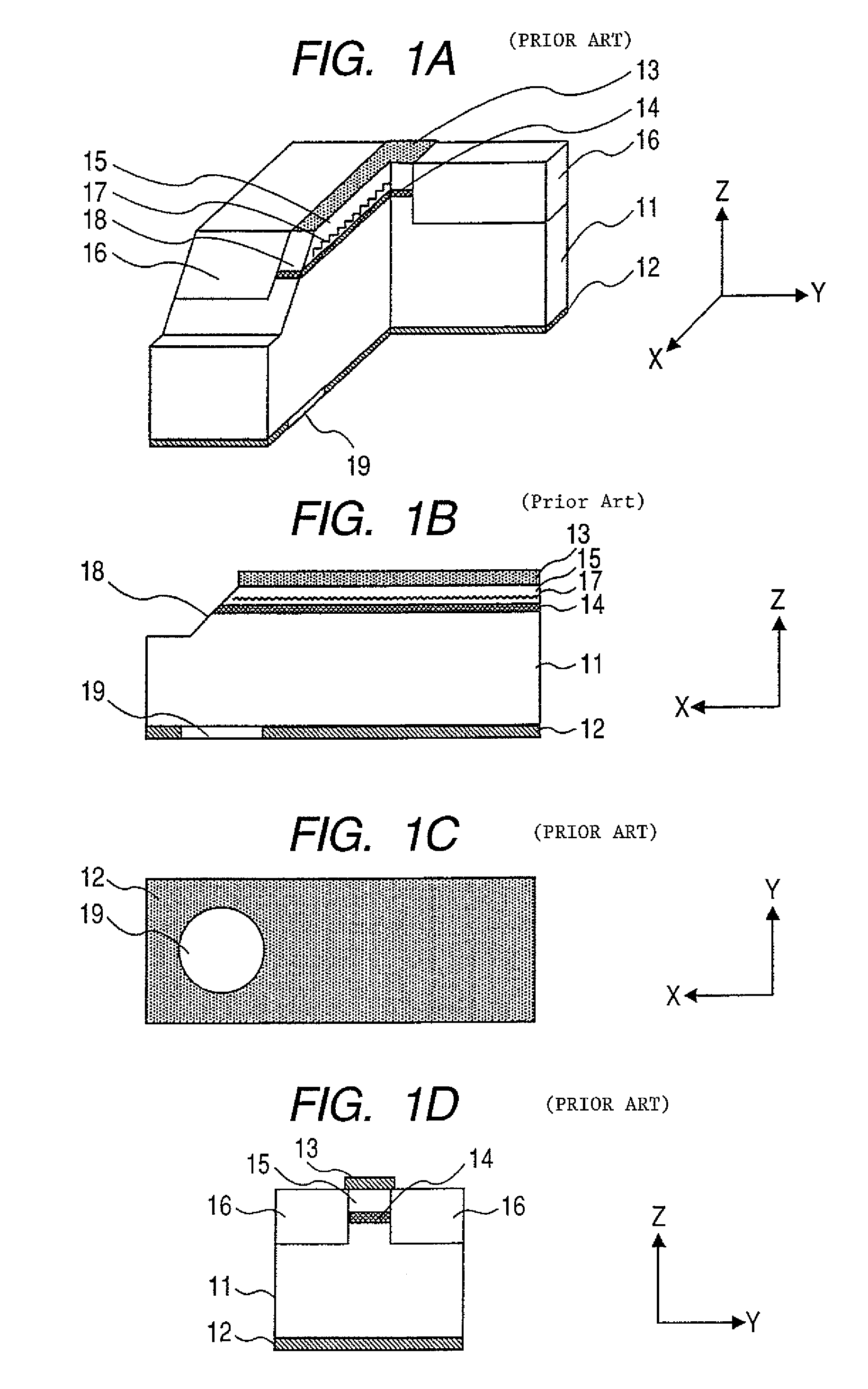
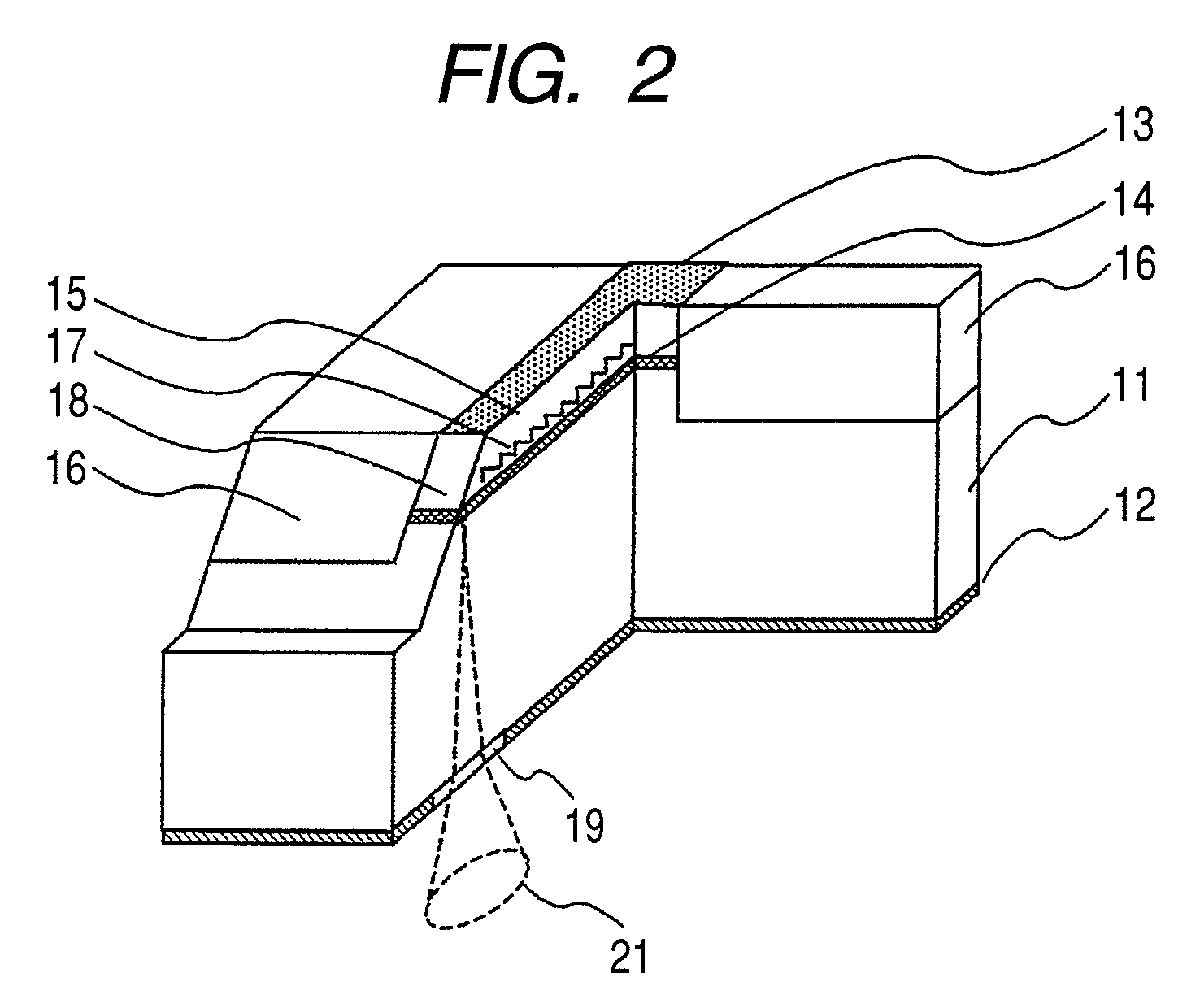
[0030]A first embodiment of the present invention will be described with reference to FIGS. 6A to 6D and 7A to 7G. This embodiment is directed to an InGaAlAs quantum well horizontal cavity surface emitting laser of 1.3 μm wavelength. FIG. 6A is a perspective view showing a cross section according to the first embodiment. FIG. 6B is a cross-sectional view of a plane that is in parallel to the beam traveling direction. FIG. 6C is a diagram showing a lower surface of the device. FIG. 6D is a cross-sectional view showing a plane that crosses the beam traveling direction. FIGS. 7A to 7G are cross-sectional views showing a process of manufacturing the device. As shown in FIGS. 6A and 6D, the optical waveguide of the device is processed into a stripe configuration, and has a buried hetero (BH) structure. This structure has been well known. In this example, a high-resistant iron-doped semi-insulated InP 16 is buried in the periphery of the stripe-shaped optical waveguide in the buried heter...

second embodiment

[0043]A second embodiment of the present invention will be described with reference to FIGS. 8A to 8D, 9A to 9E, and 10. This embodiment is directed to an InGaAsP quantum well horizontal cavity surface emitting laser having a wavelength of 1.3 μm band. FIG. 8A is a perspective view showing a cross section according to the second embodiment of the present invention. FIG. 8B is a cross-sectional view of a plane that is in parallel to the beam traveling direction. FIG. 8C is a diagram of a lower surface of the device. FIG. 9D is a cross-sectional view of a plane that crosses the beam traveling direction. FIGS. 9A to 9E are cross-sectional views showing a device manufacturing process. As shown in FIGS. 8A and 8D, the optical waveguide of the device is processed in the form of a stripe, and has a buried hetero structure. In this example, a ruthenium doped high-resistant semi-insulated InP 16 is buried in the periphery of the optical waveguide in the form of a stripe in the buried hetero ...

third embodiment

[0053]A third embodiment of the present invention will be described with reference to FIG. 12. This embodiment is directed to an example in which the semiconductor laser of the present invention is applied to an optical module used as a terminal of wavelength division multiplexing transmission that transmits beams of plural wavelengths by means of one optical fiber, or single-conductor bi-directional optical transmission.

[0054]In the configuration of FIG. 12, there are disposed an optical device mounted substrate 122 on which the laser device 101 and the photodiode 121 according to the present invention are mounted on a line in a lateral direction of the substrate front surface, respectively, a first optical functions integrated substrate 124 having an angle with respect to the substrate parallel on one plane of the substrate, and providing a first inclined plane 123 for refracting the beam that propagates in a direction of the substrate thickness, and a second optical functions int...


PUM


Abstract

In a horizontal cavity surface emitted laser, there is provided a device structure that is capable of obtaining a circular narrow-divergence emitted beam that is high in the optical coupling efficiency with a fiber. As a first means, there is provided a horizontal cavity surface emitting laser having a structure in which the plane mirror that is inclined by 45° and the bottom lens of the oval configuration are integrally structured. As a second means, there is provided a horizontal cavity surface emitting laser in which the mirror having the columnar front surface configuration inclined by 45° and the bottom lens of the columnar front surface configuration are integrally structured. Since the horizontal component and the vertical component of the laser beam can be shaped, independently, through the above means. As a result, it is possible to obtain the circular narrow-divergence emitted beam.

Description

CLAIM OF PRIORITY[0001]The present application claims priority from Japanese application JP 2007-117393 filed on Apr. 26, 2007, the content of which is hereby incorporated by reference into this application.FIELD OF THE INVENTION[0002]The present invention relates to semiconductor lasers such as lasers for optical communication systems or lasers for optical disc systems, and an optical module such as an optical transceiver module or a can module into which the semiconductor laser is incorporated.BACKGROUND OF THE INVENTION[0003]The semiconductor lasers are classified into the following three kinds of semiconductor lasers according to the combination of the cavity direction and the laser beam emitting direction. A first semiconductor laser is a horizontal cavity edge emitting laser, a second semiconductor laser is a vertical cavity surface emitting laser, and a third semiconductor laser is a horizontal cavity surface emitting laser. The first horizontal cavity edge emitting laser is ...

Claims


Application Information

Patent Timeline
Patent Type & Authority Patents(United States)
IPC IPC(8): H01S3/08H01S5/00H01S5/12H01S5/185
CPCB82Y20/00G02B6/4246H01S5/18G02B6/4214H01S5/005H01S5/02212H01S5/02248H01S5/02284H01S5/026H01S5/0267H01S5/028H01S5/1085H01S5/12H01S5/2224H01S5/2275H01S5/34306H01S5/02325H01S5/02251H01S5/185
Inventor SHINODA, KAZUNORIADACHI, KOICHIROARIMOTO, HIDEO
Owner LUMENTUM JAPAN INC
Why Eureka
Try Eureka