Dual storage node pixel for CMOS sensor

Inactive Publication Date: 2007-10-23
TELEDYNE DIGITAL IMAGING INC
View PDF17 Cites 71 Cited by
  • Summary
  • Abstract
  • Description
  • Claims
  • Application Information

AI Technical Summary

Benefits of technology

[0009]It is an object to the present invention to overcome limitation of the prior art. This and other objects are achieved in a sensor that includes control circuitry and a pixel. The pixel includes a photo site, a first storage node and a second storage node. The control circuitry causes the pixel to transfer a first collected sign

Problems solved by technology

There may be some disadvantages that arise from the time delay between collecting two frames of data.
Any change in ligh

Method used


Image

  • Dual storage node pixel for CMOS sensor
  • Dual storage node pixel for CMOS sensor
  • Dual storage node pixel for CMOS sensor

Examples


first embodiment

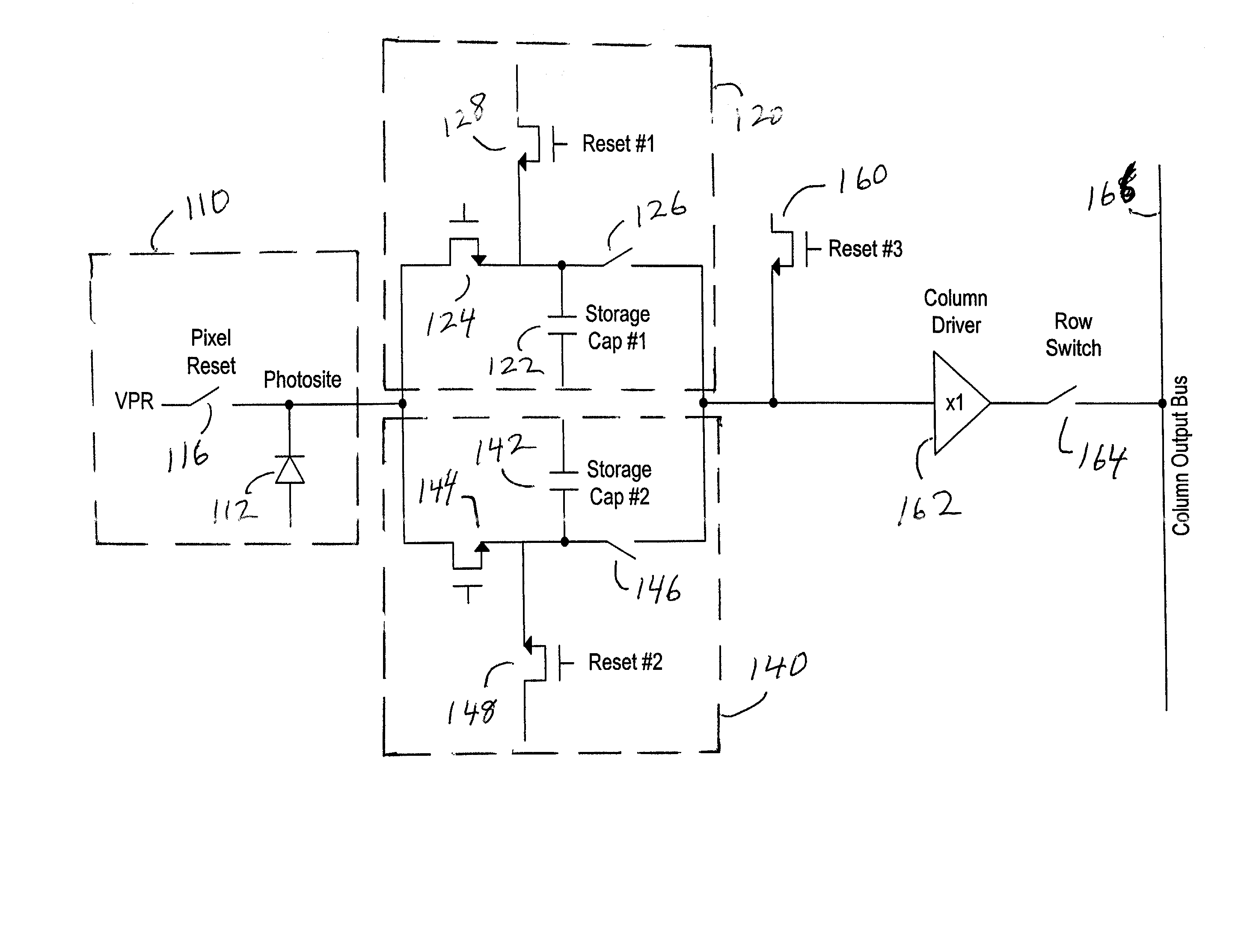
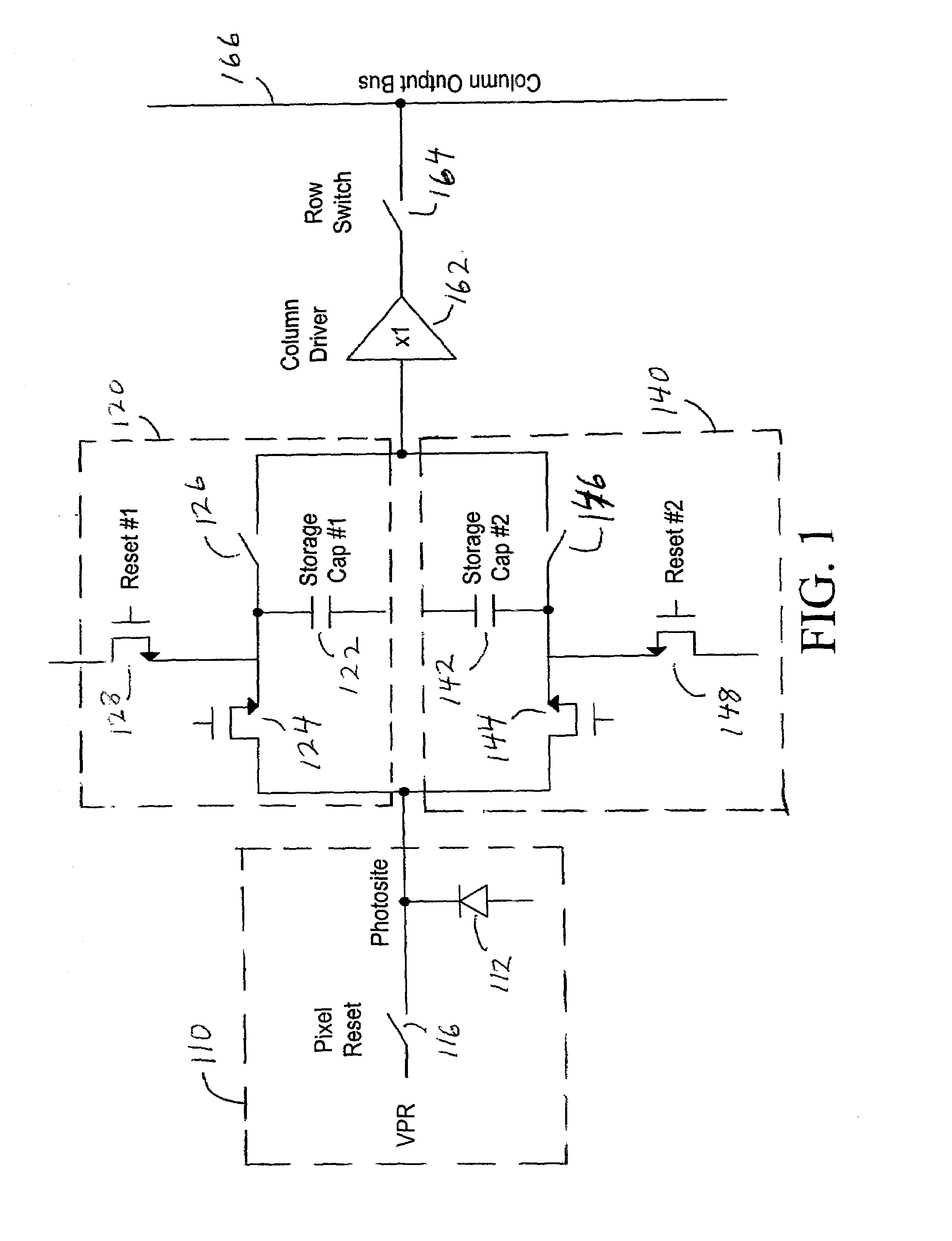
[0021]In the invention, a sensor includes control circuitry and a pixel having a photo site (110 of FIG. 1, 210 of FIG. 2), a first storage node (120 of FIG. 1, 220 of FIG. 2) and a second storage node (140 of FIG. 1, 240 of FIG. 2). As will be appreciated from the disclosure herein, the control circuitry transfers a first collected signal from the photo site to the first storage node during a first period, transfers a second collected signal from the photo site to the second storage node during a second period that follows the first period, and then transfer the first and second collected signals out of the pixel during a third period that follows the second period.

[0022]FIG. 1 illustrates the charge transfer architecture. Signal charge is transferred from the photosite across two separate transfer gates to two separate storage capacitors. In another embodiment of the invention, in the sensor described above, the photo site (110) includes a photo detector (112) where the photo dete...

second embodiment

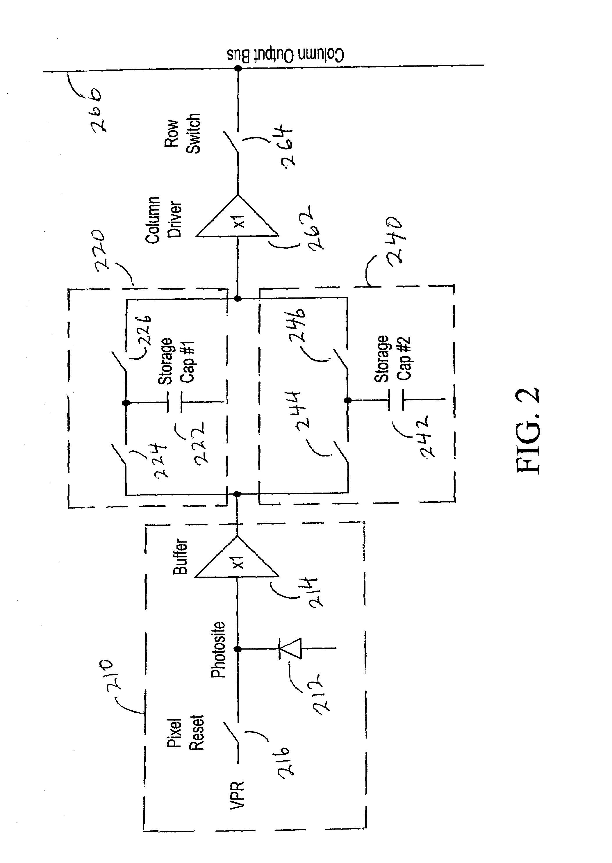
[0027]FIG. 2 illustrates the buffered photosite architecture. Signal charge is converted to a voltage on the photosite which is then buffered and directed onto one of two sample-and-hold capacitors. In the invention, a sensor includes control circuitry and a pixel having a photo site (210 of FIG. 2), a first storage node (220 of FIG. 2) and a second storage node (240 of FIG. 2). As will be appreciated from the disclosure herein, the control circuitry transfers a first collected signal from the photo site to the first storage node during a first period, transfers a second collected signal from the photo site to the second storage node during a second period that follows the first period, and then transfer the first and second collected signals out of the pixel during a third period that follows the second period. The photo site (210) includes a photo detector (212) and an input buffer (214) where the photo detector is either a photodiode or a pinned photodiode. The first and second c...


PUM


Abstract

A sensor includes control circuitry and a pixel. The pixel includes a photo site, a first storage node and a second storage node. The control circuitry causes the pixel to transfer a first collected signal from the photo site to the first storage node during a first period, to transfer a second collected signal from the photo site to the second storage node during a second period that follows the first period, and to transfer the first and second collected signals out of the pixel during a third period that follows the second period.

Description

[0001]The priority benefit of the Jun. 5, 2001 filing date of provisional application 60 / 295,554 is hereby claimed.BACKGROUND OF THE INVENTION[0002]1. Field of the Invention[0003]The present invention relates to a dual storage node pixel for a CMOS sensor. In particular, the invention relates to use of the two storage nodes for subtraction of background illumination.[0004]2. Description of Related Art[0005]In a conventional CMOS imager, a photo generated signal in a pixel is integrated for a period of time and then subsequently read out. Generally, in some sensors, a single frame (an array of pixels) is collected and then read out before the collection of the subsequent frame. Also, in other sensors, a single frame (an array of pixels) is collected during an integration period that overlaps a period where the previously collected frame of pixels is being read out. There may be some disadvantages that arise from the time delay between collecting two frames of data.[0006]For example, ...

Claims


Application Information

Patent Timeline
IPC IPC(8): H04N3/14H01L31/062H01L31/113H04N5/335H04N5/353H04N5/374
CPCH04N5/335H04N5/37452H04N5/374H04N25/00H04N25/771H04N25/76
Inventor WEALE, GARETH P.SMITH, CHARLES R.FOX, ERIC C.DYKAAR, DOUGLASSONDER, MATTHIASLI, BINQIAO
Owner TELEDYNE DIGITAL IMAGING INC
Why Eureka
Try Eureka