Method of fabricating a high-layer-count backplane

Inactive Publication Date: 2005-02-03
DELL MARKETING CORP
View PDF32 Cites 17 Cited by
  • Summary
  • Abstract
  • Description
  • Claims
  • Application Information

AI Technical Summary

Benefits of technology

This disclosure describes an electrical router backplane that overcomes many of the electrical and mechanical limitations of large prior art electrical backplanes, and methods for its design and fabrication. Generally, this backplane comprises multiple high-speed signaling layers of differential signaling pairs, separated by ground layers. Preferably, power distribution layers and/or low-speed signaling layers are em

Problems solved by technology

With any appreciable number of cards, it becomes infeasible to build large parallel point-to-point connection buses between each pairing of the cards.
This limitation hinders further growth in large router throughput, a

Method used


Image

  • Method of fabricating a high-layer-count backplane
  • Method of fabricating a high-layer-count backplane
  • Method of fabricating a high-layer-count backplane

Examples


Example

1 Definitions

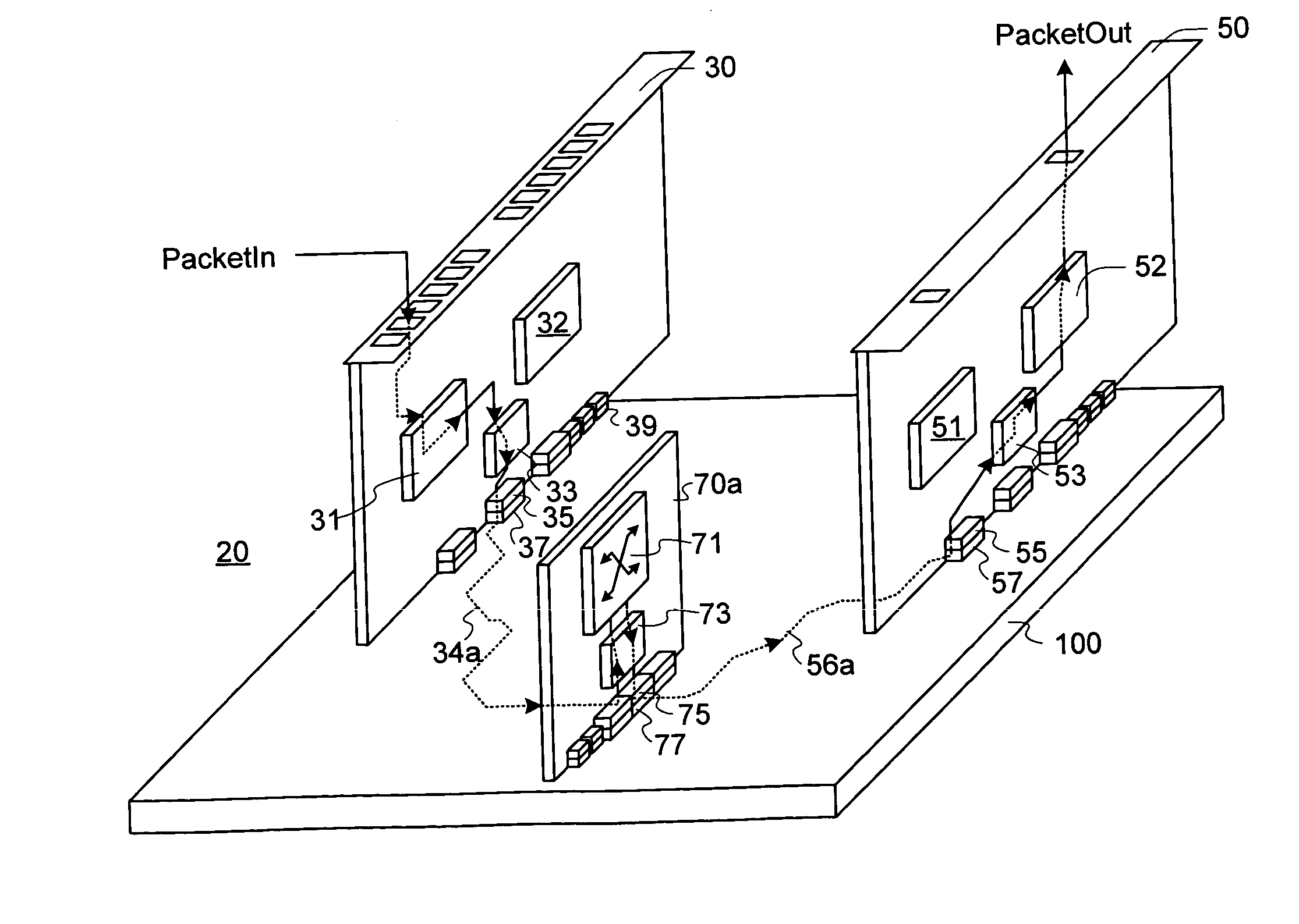
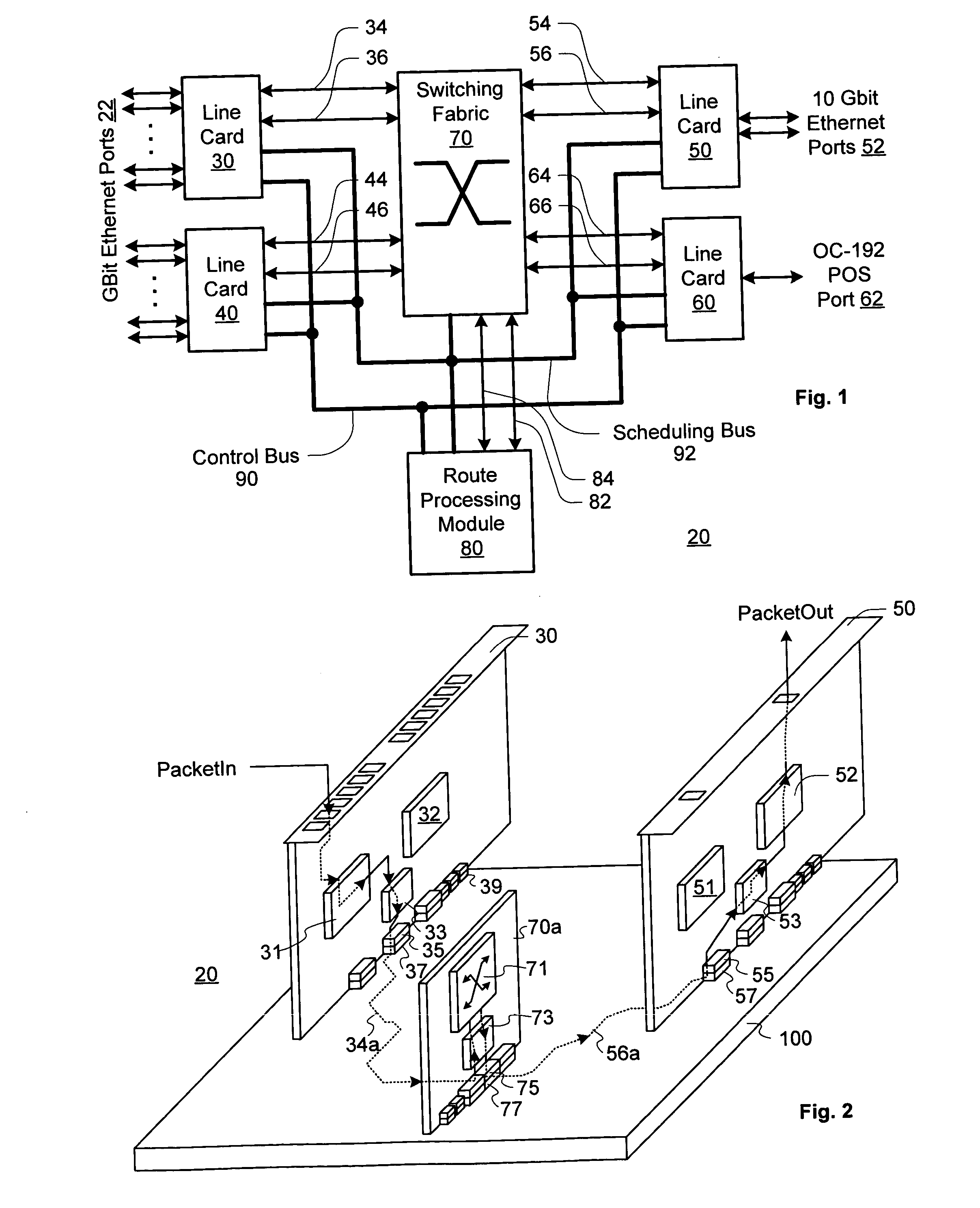
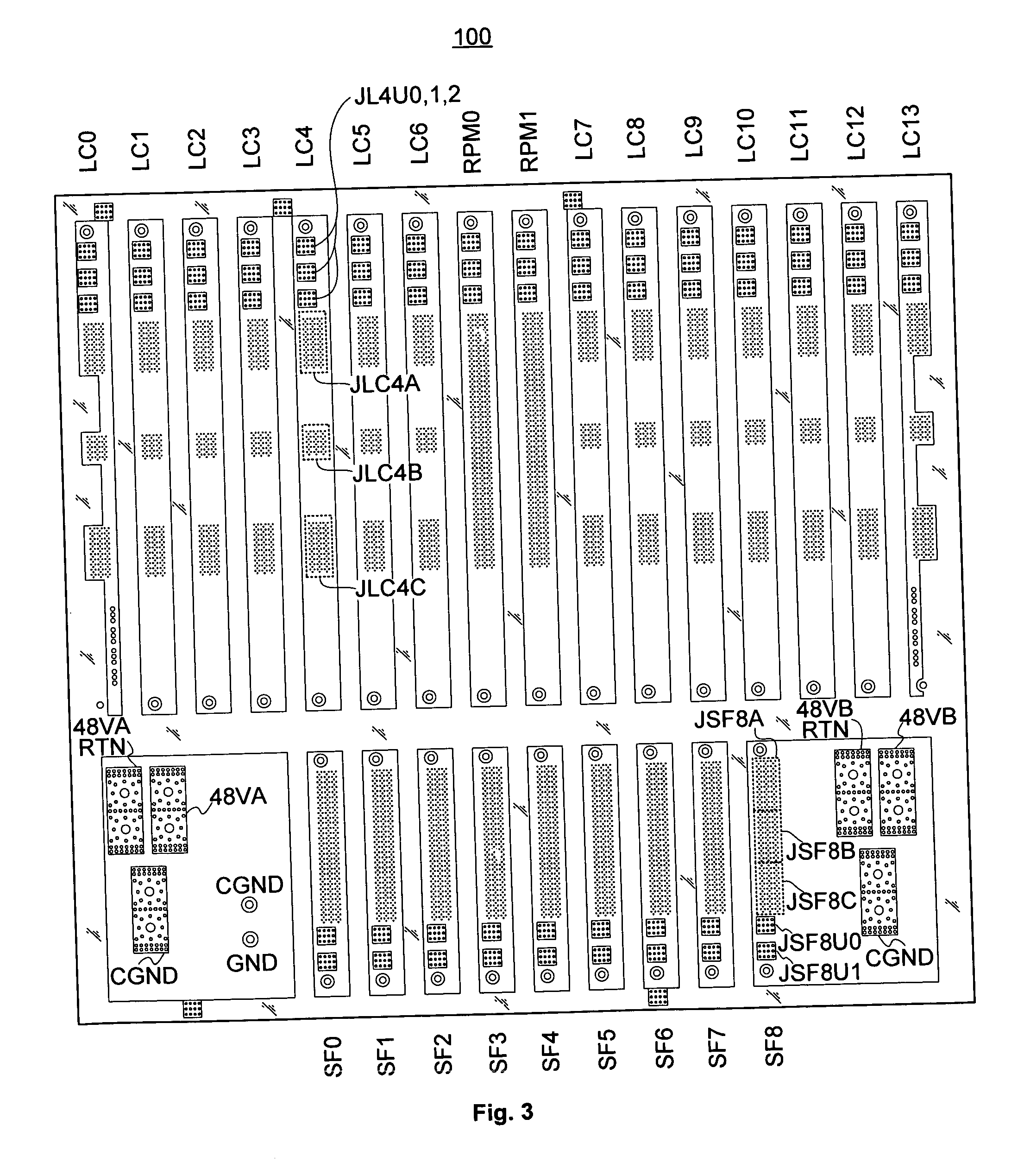
Several terms have been assigned particular meanings within the context of this disclosure. As used herein, high speed signaling refers to signaling on a differential signal pair at a data rate greater than about 2.5 Gbps. A high-speed signaling layer or high-speed differential trace plane contains high-speed differential signal trace pairs, but may also contain lower speed and / or single-ended traces. A core dielectric layer is one that is cured and plated prior to assembly of a circuit board. A b-stage dielectric layer is one that is cured during assembly of cores into the circuit board. Differential signaling (or balanced signaling) is a mode of signal transmission, using two conductors, in which each conductor carries a signal of equal magnitude, but opposite polarity. Single-ended signaling (or unbalanced signaling) is a mode of signal transmission where one conductor carries a signal with respect to a common ground. The impedance of a differential trace is more ...


PUM

PropertyMeasurementUnit
Dielectric polarization enthalpyaaaaaaaaaa
Speedaaaaaaaaaa
Electrical conductoraaaaaaaaaa

Abstract

The disclosed board fabrication techniques and design features enable the construction of a reliable, high-layer-count, and economical backplane for routers and the like that require a large number of signaling paths across the backplane at speeds of 2.5 Gbps or greater, as well as distribution of significant amounts of power to router components. The disclosed techniques and features allow relatively thick (e.g., three- or four-ounce copper) power distribution planes to be combined with large numbers of high-speed signaling layers in a common backplane. Using traditional techniques, such a construction would not be possible because of the number of layers required and the thickness of the power distribution layers. The disclosed embodiments use novel layer arrangements, material selection, processing techniques, and panel features to produce the desired high-speed layers and low-noise high-power distribution layers in a single mechanically stable board.

Description

FIELD OF THE INVENTION This invention relates generally to high-layer-count circuit board fabrication, and more specifically to methods for constructing backplane wiring systems for highly interconnected, high-speed modular digital communications systems such as routers and switches. BACKGROUND OF THE INVENTION A backplane generally comprises a printed circuit board having a number of card connection slots or bays. Each slot or bay comprises, e.g., one or more modular signal connectors or card edge connectors, mounted on the backplane. A removable circuit board or “card” can be plugged into the connector(s) of each slot. Each removable circuit board contains drivers and receivers necessary to communicate signals across the backplane with corresponding drivers and receivers on other removable circuit boards. One or more layers of conductive traces are formed on and / or in the backplane. The traces connect to individual signal connection points at the various slots to form data line...

Claims


Application Information

Patent Timeline
IPC IPC(8): H05K1/02H05K1/11H05K3/38H05K3/42H05K3/46
CPCH05K1/0218Y10T29/49162H05K1/0243H05K1/0271H05K1/116H05K3/382H05K3/429H05K3/4626H05K3/4641H05K3/4688H05K2201/0209H05K2201/044H05K2201/0723H05K2201/09236H05K2201/093H05K2201/09309H05K2201/09318H05K2201/09354H05K2201/09381H05K2201/09454H05K2201/09636H05K2201/09663H05K2201/09718H05K2201/09781H05K2203/061H05K2201/09327Y10T29/49163Y10T29/49128Y10T29/49156Y10T29/49155Y10T29/49165Y10T29/49117H05K1/024
Inventor GOERGEN, JOEL R.
Owner DELL MARKETING CORP
Why Eureka
Try Eureka