Signal testing of integrated circuit chips

a technology of integrated circuits and signal testing, which is applied in the field of integrated circuits, can solve the problems of most commonly encountered noise problems in high-speed systems, difficult ic design, board layout and pcb manufacture, and computer systems that are more susceptible to electromagnetic interference, so as to facilitate and autonomously detect ground boun

Active Publication Date: 2007-10-23
VIA TECH INC
View PDF7 Cites 14 Cited by
  • Summary
  • Abstract
  • Description
  • Claims
  • Application Information

AI Technical Summary

Benefits of technology

[0007]It is an object of the present invention to provide a method of signal testing, which permits an IC chip to easily and autonomously detect ground bounce and power bounce problems.

Problems solved by technology

Although this is a common method in recent years, a great increase in the I / O density causes computer systems to be more susceptible to electromagnetic interference (EMI) caused by higher frequencies, and presents a difficult challenge in IC design, board layout and PCB manufacture.
Today, the most commonly encountered noise problems in high-speed systems are ground bounce and power bounce.
In this case, ground bounce on the LSB in the low state may be substantial enough to cross the input threshold of a subsequent device, which in turn can cause this device to misinterpret the static LSB as a logic “1”.
In this case, power bounce on the MSB in the high state may be substantial enough to drop below the input threshold of a subsequent device, which in turn can cause this device to misinterpret the static MSB as logic “0”.
Ground and power bounce problems can result in the unexpected, unreliable, and sometimes intermittent, behavior of a computer system.
As data transfer rate increases, SSO noise becomes a crucial issue for high-speed IC design.

Method used


Image

  • Signal testing of integrated circuit chips
  • Signal testing of integrated circuit chips
  • Signal testing of integrated circuit chips

Examples


Embodiment Construction

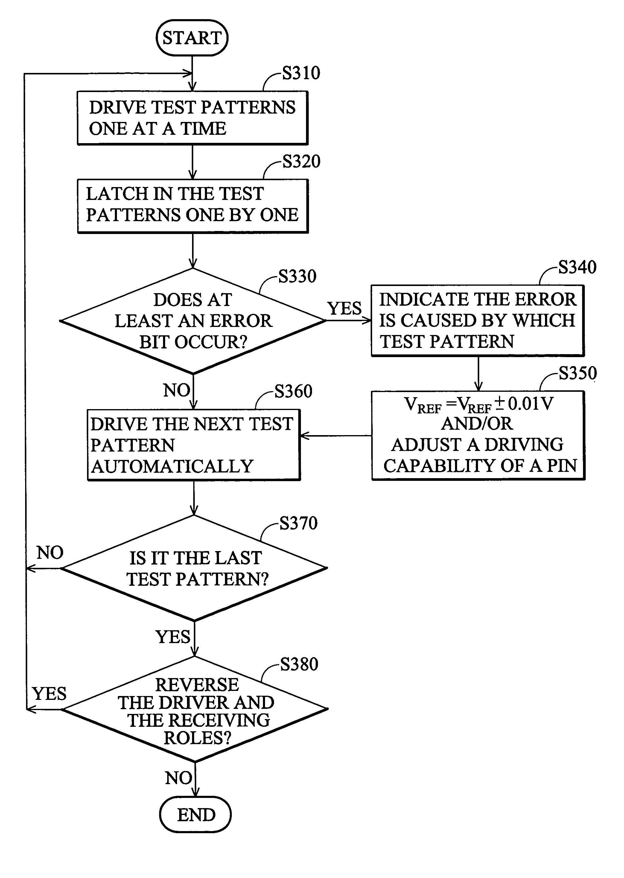
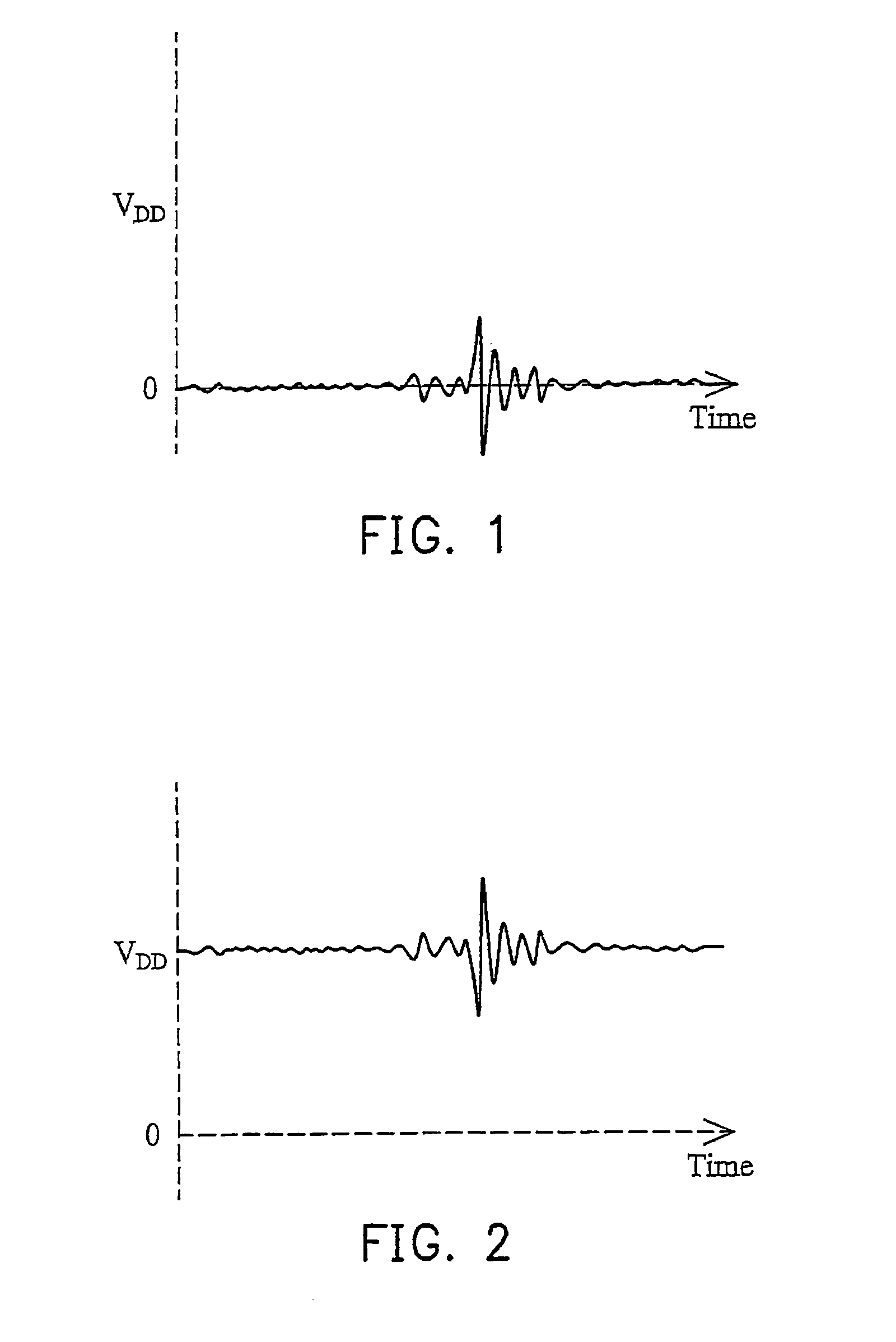
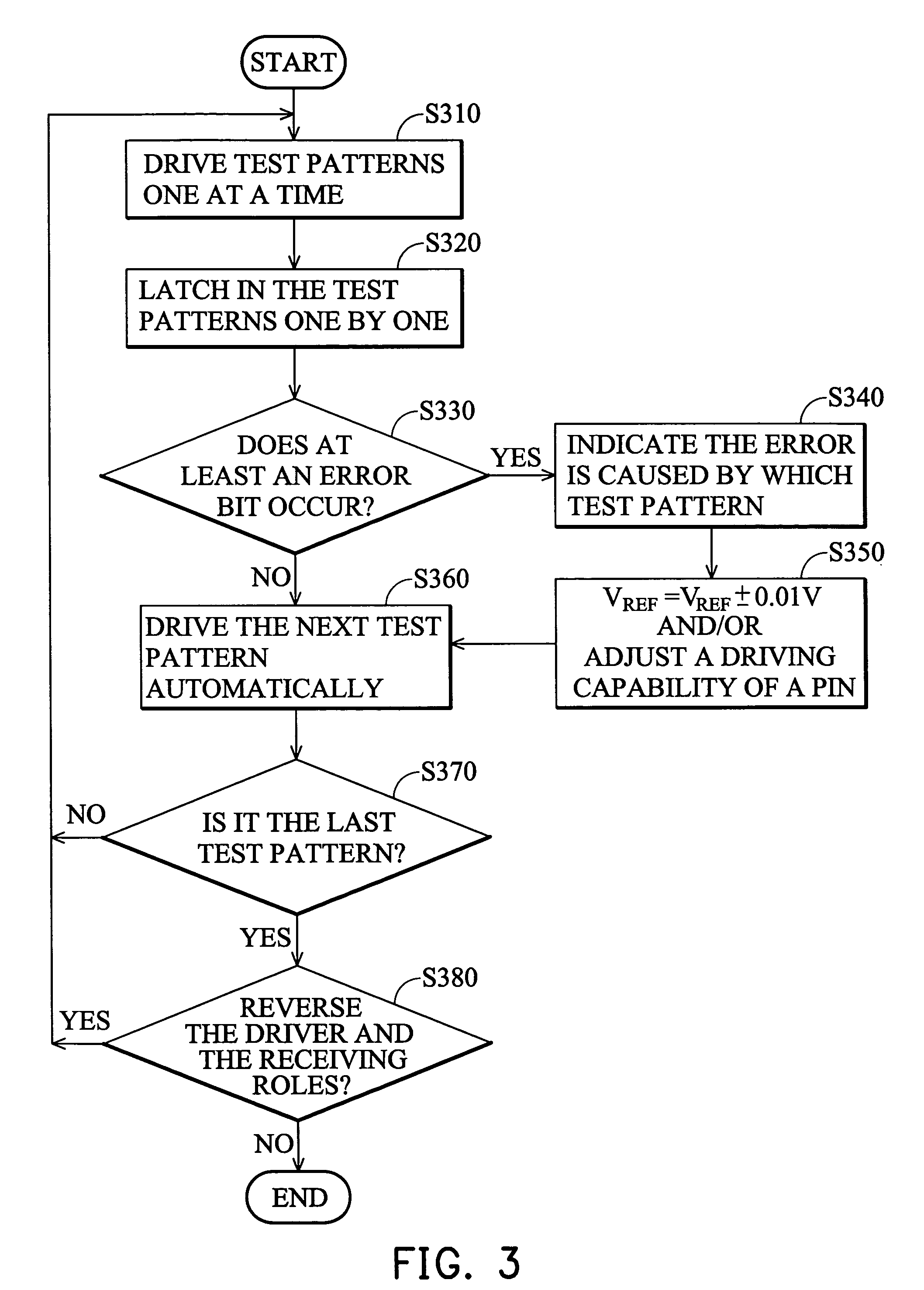
[0017]The present invention exploits fixed and predicable test patterns to generate the simultaneous switching effects on board traces between driver and receiver IC chips as well as I / O pins thereof. In this manner, the potential problems of ground bounce and power bounce between the driver and receiver IC chips can be detected accordingly. The receiver IC chip automatically changes a reference voltage level to adjust its input threshold when an error is detected. If the error still occurs, the driver IC chip can further alter its driving capability to adjust output timing thereby avoiding running into ground or power bounce.

[0018]In accordance with the invention, driver and receiver IC chips individually have three types of built-in test patterns including a ground bounce type, a power bounce type and a heavy load type to detect various noise problems. With respect to the ground bounce type, a driver IC chip drives an initial test pattern consisting of all “1” and drives the remai...


PUM


Abstract

A method for testing signals of integrated circuits (ICs). According to the invention, a first IC chip successively drives a number of test patterns one at a time. At the receiving end, a second IC chip latches in the test patterns one by one. Meanwhile, the second IC chip determines whether a currently latched test pattern is correct or not. If it is incorrect and at least an error bit occurs, depending on the type of the test patterns, the second IC chip indicates that there exists ground bounce or power bounce in a signal trace corresponding to the error bit.

Description

BACKGROUND OF THE INVENTION[0001]1. Field of the Invention[0002]The invention relates to integrated circuits, and more particularly to a mechanism for testing and fine-tuning the signal quality of integrated circuit (IC) chips.[0003]2. Description of the Related Art[0004]In computer systems, the general method for improving the data transfer rate is to raise the bus frequency or increase the data bus width. Growing bus width significantly increases the I / O density of IC chips. Although this is a common method in recent years, a great increase in the I / O density causes computer systems to be more susceptible to electromagnetic interference (EMI) caused by higher frequencies, and presents a difficult challenge in IC design, board layout and PCB manufacture.[0005]Today, the most commonly encountered noise problems in high-speed systems are ground bounce and power bounce. The basic form of ground or power bounce occurs when the IC chip has multiple output pins changing state simultaneou...

Claims


Application Information

Patent Timeline
Patent Type & Authority Patents(United States)
IPC IPC(8): G01R31/28G06F11/00G01R31/317
CPCG01R31/31709G01R31/31707
Inventor LIN, I-MINGLIU, JEN-NAN
Owner VIA TECH INC
Why Eureka
Try Eureka