Circuit for measuring on-chip power supply integrity

a power supply integrity and circuit technology, applied in resistance/reactance/impedence, digital transmission, instruments, etc., can solve problems such as ground bounce parasitic phenomenon, device failure in operation, and power supply quality on those chips becomes an issue for chip designers, and achieve the effect of removing any influence of external noise on measuremen

Inactive Publication Date: 2005-01-13
MICRON TECH INC
View PDF4 Cites 5 Cited by
  • Summary
  • Abstract
  • Description
  • Claims
  • Application Information

AI Technical Summary

Benefits of technology

[0010] The present invention provides a circuit and method for measuring power supply integrity. The circuit may be incorporated on-chip and, in fact, the circuit is small enough to be integrated many times across the surface of the die. The circuit instantaneously measures, e.g., the voltage of a power supply, which may be fluctuating at the time of measurement. In addition, the circuit isolates itself from all chip power rails for the duration of the measurement, thereby eliminating any influence of external noise on the measurement. A storage capacitor is charged up to full power rail voltage for powering up a comparator. Then, the comparator is isolated from the power rails and the measurements are taken. Based upon the measurements, certain power supply integrity parameters are quantified including ground bounce and power droop.

Problems solved by technology

As greater numbers of components are integrated onto semiconductor chips, the quality of the power supplies on those chips becomes an issue for chip designers.
A poorly designed power supply architecture can lead to devices failing in operation due to problems such as, e.g., ground bounce and power droop.
Ground bounce is a transient parasitic phenomenon that occurs in high-speed devices and is caused in part by device packaging.
The problem arises because this large current must be returned through the ground pins on the device.
This raises the ground reference voltage, which leads to decreased noise margins at receiving modules.
Lowered noise margins can result in logic values being sensed improperly, a fatal communications error.
Since the wires that connect the circuits to the power supply are not ideal and have resistance, capacitance and inductance, a sudden demand for current will lead to a voltage drop across these wires.
The inductance of the wire causes a voltage loss related to the rate of change of current demand.
A clock switching causing a sudden large current demand causes a sudden voltage drop to occur across the power supply lines on the chip.
To compound this problem, the failures are likely to be caused by dynamic effects and may not be detectable at final test which is usually performed at a much lower frequency than the typical operating frequency of the device.
Unfortunately, these tools are only as good as the models they use and, to improve their speed of operation, the models use a simplified view of the operating environment.
This simplification leads to a reduction in accuracy of the results which is sometimes unacceptable.
Furthermore, these tools do not consider packaging and board level details, both of which can have significant effects on the power supply quality.
The indirect methods tend to suffer from the fact that they cannot resolve very fast edge rates and are very expensive.
Unfortunately, it is very time consuming, hard to automate and wastes die area with probe pad landing sites.
It also suffers from the problem that performing the measurement disturbs the circuit that is being measured.

Method used


Image

  • Circuit for measuring on-chip power supply integrity
  • Circuit for measuring on-chip power supply integrity
  • Circuit for measuring on-chip power supply integrity

Examples


Embodiment Construction

[0018] The present invention will be described as set forth in exemplary embodiments described below in connection with FIGS. 1-6. Other embodiments may be realized and other changes may be made to the disclosed embodiments without departing from the spirit or scope of the present invention.

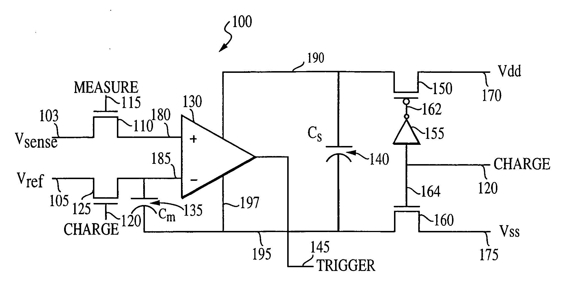
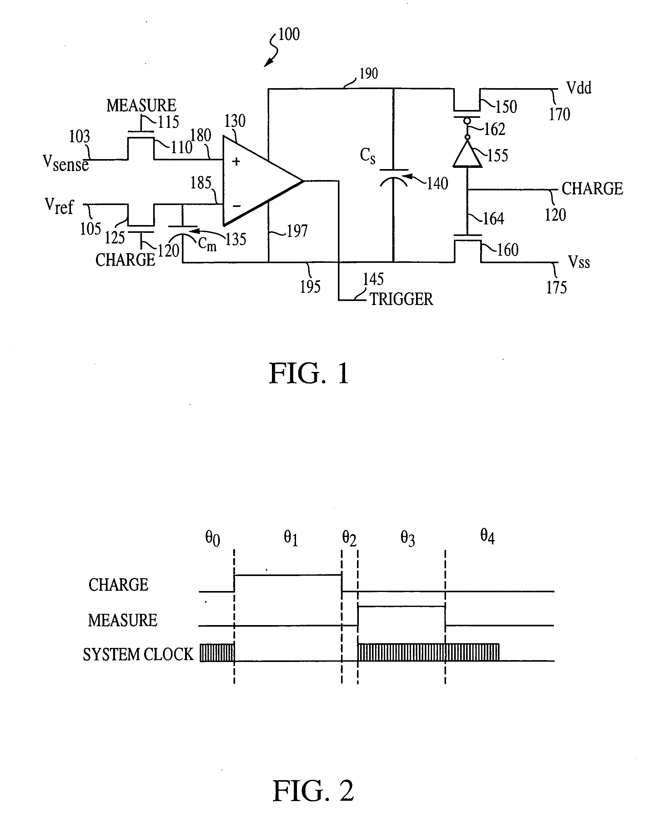
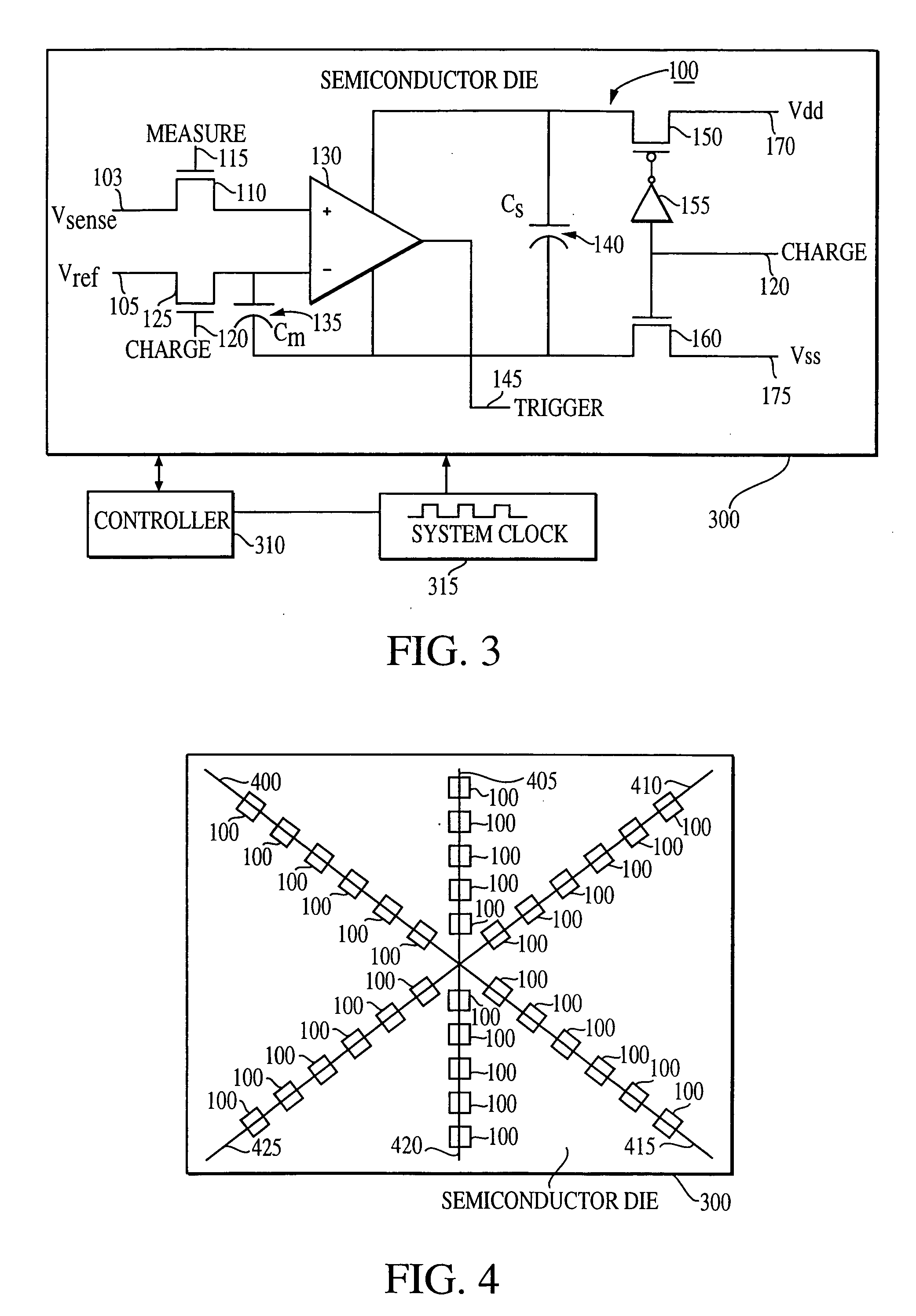
[0019] Referring now to FIG. 1, a test circuit 100 is depicted in accordance with an exemplary embodiment of the invention. In a preferred embodiment (and for purposes of this description), circuit 100 is integrated on a semiconductor chip (or die) for measuring at least one circuit parameter of a circuit under test on the semiconductor die; however, this is not a requirement for practicing the invention. Test circuit 100 includes a comparator 130 having a first input 185 (“−”) coupled to a first side of capacitor 135. Input 185 is also coupled to a first terminal of transistor 125. A second terminal of transistor 125 receives a reference voltage (Vref) at position 105. Reference voltage (Vref) ...


PUM


Abstract

A test circuit and method for measuring power supply integrity is provided. The circuit may be incorporated on-chip and is small enough to be integrated many times across the surface of the die for measuring integrity parameters at several locations on the chip. The circuit instantaneously measures, e.g., the rail voltage of a power supply, which may be fluctuating at the time of measurement. In addition, the circuit isolates itself from all chip power rails for the duration of the measurement, thereby eliminating any influence of external noise on the measurement. A storage capacitor is charged up to full power rail voltage for powering up a comparator. Then, the comparator is isolated from the power rails and the measurements are taken. Based upon the measurements, certain power supply integrity parameters are quantified including ground bounce and power droop.

Description

BACKGROUND OF THE INVENTION [0001] 1. Field of the Invention [0002] The present invention relates to integrated circuits. More specifically, it relates to a circuit for measuring power integrity of a chip containing integrated circuits. [0003] 2. Description of Prior Art [0004] As greater numbers of components are integrated onto semiconductor chips, the quality of the power supplies on those chips becomes an issue for chip designers. A poorly designed power supply architecture can lead to devices failing in operation due to problems such as, e.g., ground bounce and power droop. [0005] Ground bounce is a transient parasitic phenomenon that occurs in high-speed devices and is caused in part by device packaging. When several I / O pins are switched simultaneously at high slew rates (which is, of course, common when driving a bus), the sum of the driving currents through each I / O pin can be quite substantial. The problem arises because this large current must be returned through the grou...

Claims


Application Information

Patent Timeline
Patent Type & Authority Applications(United States)
IPC IPC(8): G01R19/165G01R31/28H04L1/22
CPCG01R19/16552H04L1/22G01R31/2884
Inventor CORR, WILLIAM E.
Owner MICRON TECH INC
Why Eureka
Try Eureka