Unlock instant, AI-driven research and patent intelligence for your innovation.

Ion beam processing system and ion beam processing method

a technology of ion beam and processing system, which is applied in the field of ion beam processing system and ion beam processing (milling) method, can solve the problems of interlayer short circuit, difficult liftoff, and loss of inherent functions of the device, so as to achieve remarkable improvement and suppress the appearance of burrs at the mask side wall.

Inactive Publication Date: 2007-10-30
NAT INST OF ADVANCED IND SCI & TECH +1
View PDF5 Cites 0 Cited by
  • Summary
  • Abstract
  • Description
  • Claims
  • Application Information

AI Technical Summary

Benefits of technology

The present invention provides an ion beam processing system and method that prevents or suppresses burrs from forming on a mask pattern and processed surface. This is achieved by applying an electric field to the processed sample using an electrode, which deflects the atoms of the processed sample in the direction of the ion beam incidence. This results in a reduction of burrs, which can cause short-circuits, improve liftoff, and allow for processing of microdevices. Additionally, the invention eliminates the need for tilted sample surfaces and tapering of processed sectional profiles.

Problems solved by technology

These burrs 321 deposit at the side faces of the processed surfaces, so when etching a multilayer film, easily cause interlayer short-circuits and cause the inherent functions of the device to be lost, for example, see Japanese Unexamined Patent Publication (Kokai) No. 11-289058; Hiroshi GOHEI and Sotaro EISHO ed., Vacuum, vol.
That is, liftoff will become difficult.
If the size of the device is on the submicron order, the ratio of the burr 321 in the contact hole part will become remarkably high and make formation of an opening difficult.
As explained above, in the ion milling of the related art, due to burrs formed at the timing of milling (redeposition of sputtered particles), the microprocessing capability was limited.
It is becoming difficult to answer the demands for further miniaturization to the submicron and nanometer (mm) order required for future production of semiconductor devices, micro electro mechanical systems (HEMS), etc.
Further, the problem arises of increased tapering at the cross-sectional profile of the milling.

Method used


Image

  • Ion beam processing system and ion beam processing method
  • Ion beam processing system and ion beam processing method
  • Ion beam processing system and ion beam processing method

Examples


first embodiment

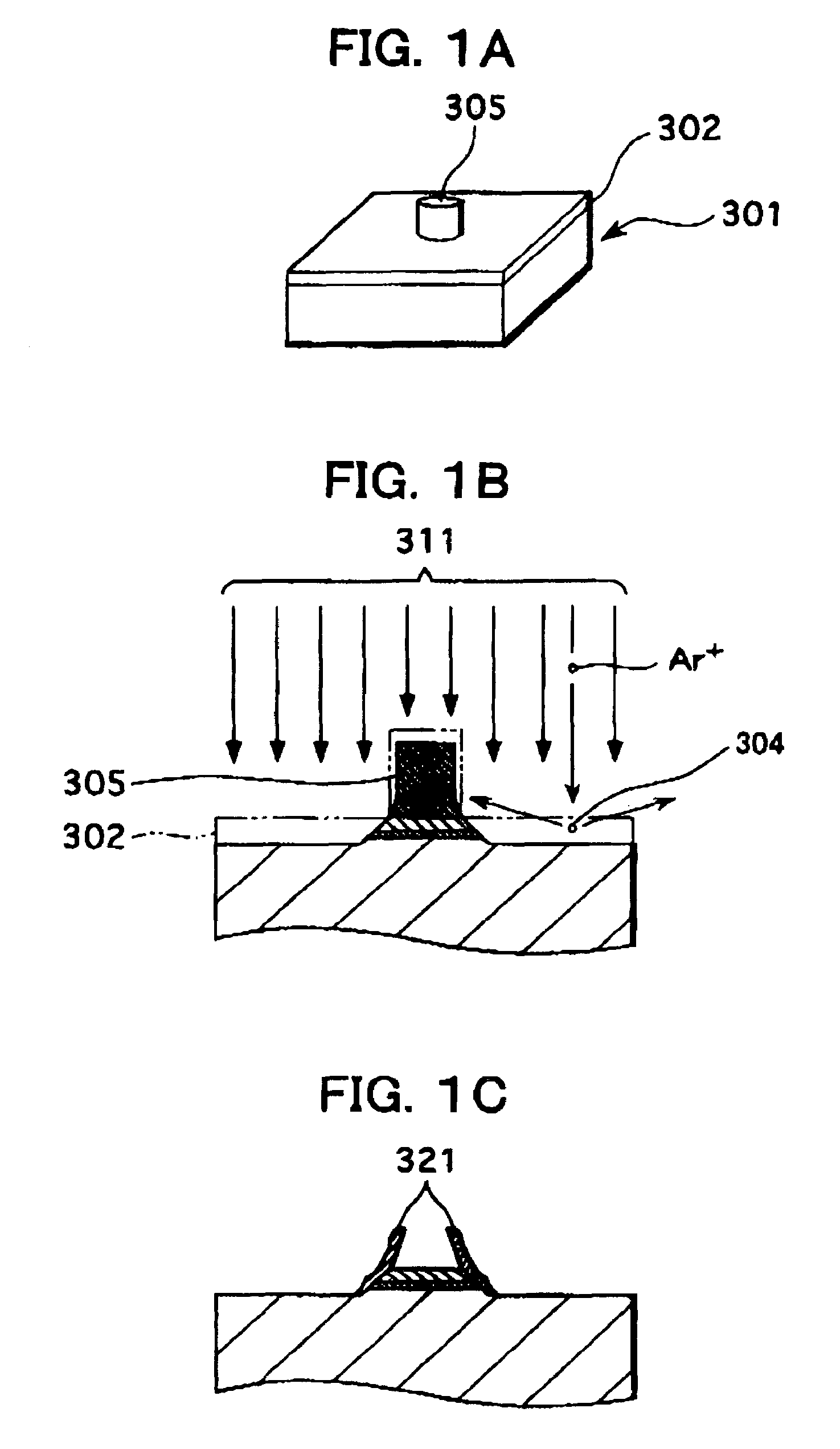
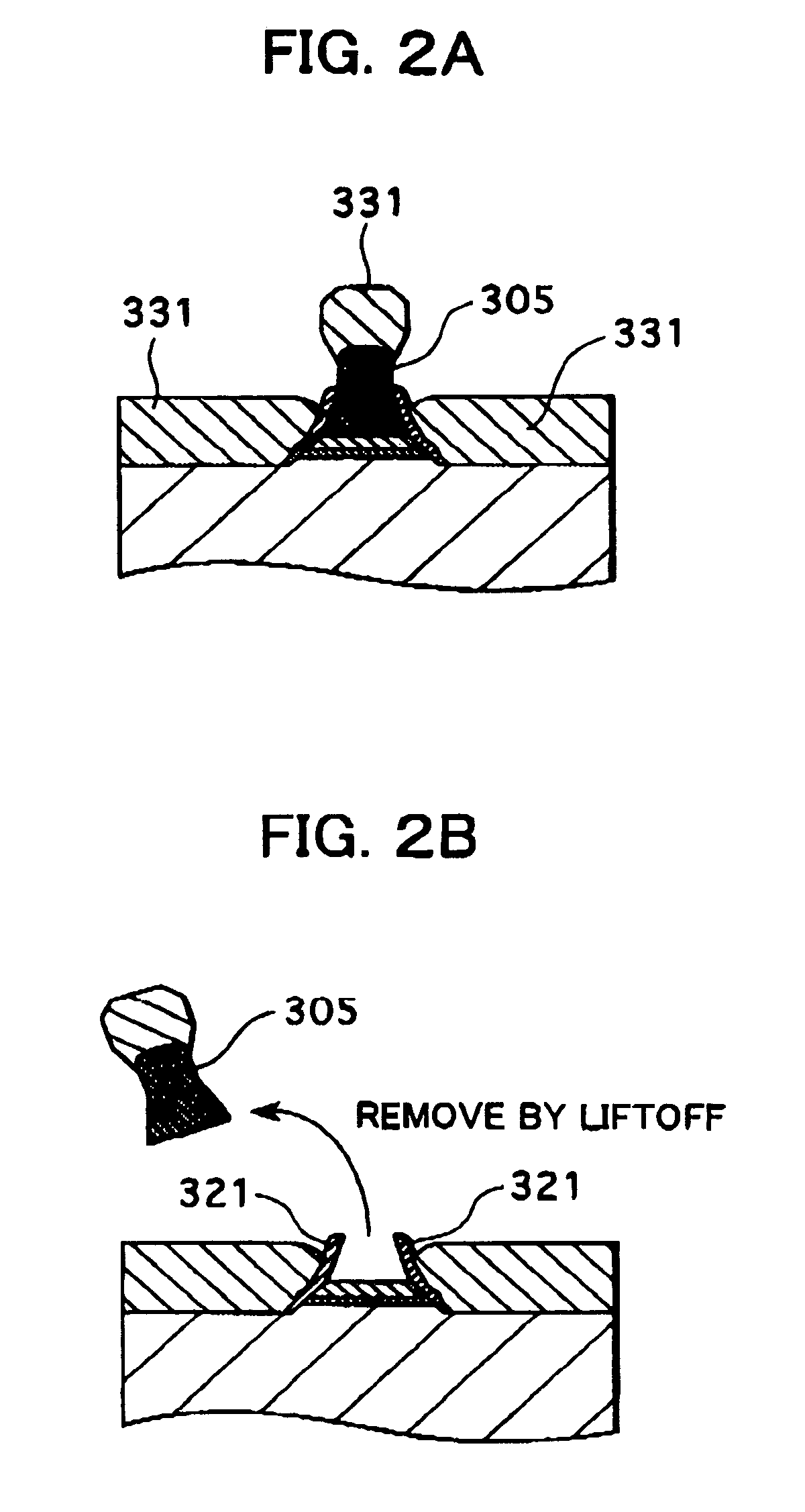
[0048]An ion beam processing system and ion beam processing method according to a first embodiment of the present invention will be described with reference to the schematic view of the configuration of FIG. 4, the perspective view of principal parts of FIG. 5, the view of the configuration of principal parts for explaining the operation of FIG. 6, etc. There are various types of ion beam processing systems, but in FIG. 4, an example of application of the present invention to a general ion beam processing system will be shown.

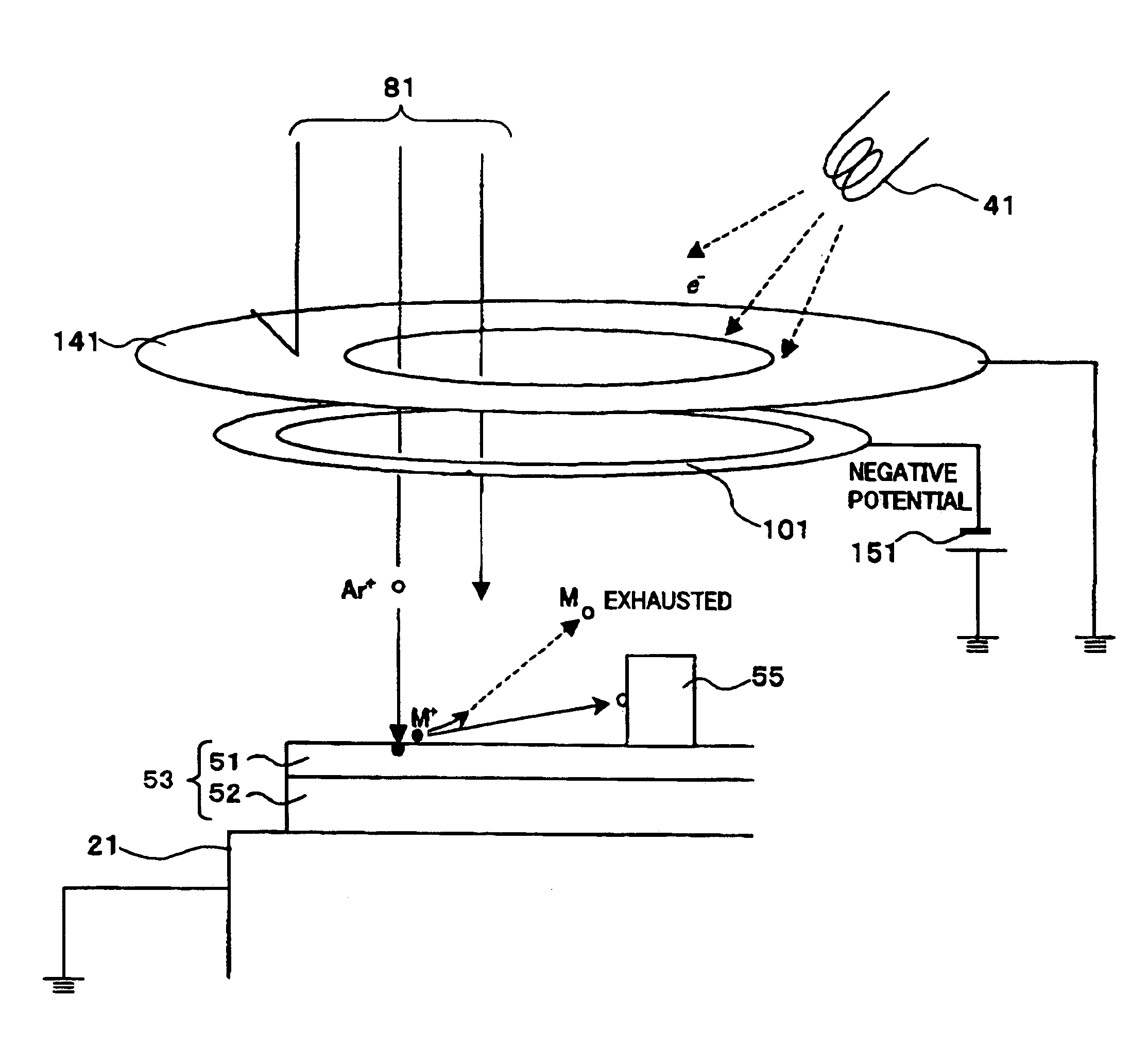
[0049]As shown in FIG. 4, the ion beam processing system 1 is provided with a vacuum chamber 11. The vacuum chamber 11 is provided inside it with a stage 21 for holding a processed sample 51. This stage 21 is designed to rotate by a not shown rotational drive device.

[0050]The vacuum chamber 11 also has arranged inside it an ion source 31 facing the processed surface of the processed sample 51 held at the stage 21. This ion source 31 for example converts introdu...

second embodiment

[0081]Next, the shape of the electrode will be explained by the schematic perspective views of configuration of FIGS. 15A to 15C. In the above embodiment, the electrode used was made a ring-shaped one, but it is also possible to use various other shapes of electrodes of good efficiency in accordance with the size of the sample substrate and the processed area. FIGS. 15A to 15C show cases of arrangement or the electrode outside of the processed sample.

[0082]As shown in FIG. 15A, a ring- and plate-shaped electrode 111a is arranged above the processed sample 51 so as not to block the ion beam 81 fired at the processed sample 51. Further, as shown in FIG. 15B, it is also possible to arrange a plurality of plate-shaped electrodes 101b at the sides of the processed sample 51.

[0083]In this figure, the example of arranging two plate-shaped electrodes 101b symmetrically across the processed sample 51 is shown, but it is also possible to arrange three or four electrodes around it. In this cas...

third embodiment

[0084]Next, the position of arrangement of the electrode (position relative to processed sample in direction of incidence of ion beam) will be explained with reference to the schematic view of the configuration of FIGS. 16A to 16D. Here, the case is shown of the arrangement of a ring-shaped electrode at the outside of the processed sample 51. Note that even in the case of plate-shad electrodes and chip-shaped electrodes, arrangement in a positional relationship with respect to the processed sample similar to that of the ring-shaped electrode is possible. Note that the arrow from the processed sample 51 to the electrode 101 in FIGS. 16B to 16D shows the electrical force lines.

[0085]As shown in FIGS. 16A and 16B, the electrode 101 can be arranged above the processed surface of the processed sample 51 (side of incidence of ion beam 81) so as to enable the ion beam 81 to pass through the inside part of the electrode 101. In this case, it is preferable that it be arranged so that the cen...


PUM


Abstract

An ion beam processing system emitting an ion beam at a workpiece to process the workpiece, provided with an electrode for applying an electric field to the workpiece, the potential of the electrode being made 0V or a negative potential, and a cover insulated from the electrode arranged at an ion beam incidence side of the electrode, thereby preventing or suppressing sputtered particles from redepositing on a master pattern and the processed surface to form burrs, and an ion beam processing method used with the same.

Description

RELATED APPLICATION DATA[0001]The present application claims priority to Japanese Application(s) No(s). P2003-373365 filed Oct. 31, 2003, which application(s) is / are incorporated herein by reference to the extent permitted by law.BACKGROUND OF THE INVENTION[0002]1. Field of Invention[0003]The present invention relates to an ion beam processing (milling) system and ion beam processing (milling) method, enabling the prevention of redeposition of sputtered particles on a mask pattern and processed surface.[0004]2. Description of the Related Art[0005]As a technique for microprocessing a thin film, a beam processing is known. This beam processing is a processing method emitting (or exposing) an argon (Ar) beam or other beam on a sample at a high speed so as to shave off parts of the sample surface. As that beam processing, ion milling using Ar ions, reactive ion etching (RIE) using also chemical reactions, etc. are known.[0006]Ion milling will be explained briefly first using FIGS. 1A to...

Claims


Application Information

Patent Timeline
Patent Type & Authority Patents(United States)
IPC IPC(8): C23C14/34C23F1/00G21K5/04G11B5/31H01J37/30H01J37/305H01L21/302H05H1/24
CPCH01J37/3053H01J2237/022
Inventor FUKUSHIMA, AKIOYAGAMI, KOJIRO
Owner NAT INST OF ADVANCED IND SCI & TECH