Image forming apparatus and image forming method

a technology of image forming apparatus and forming method, which is applied in the direction of instruments, printing, visual presentation, etc., can solve the problems of reducing the brightness of organic el elements with use, difficult to realize an apparatus that outputs a high quality image, and difficult to produce organic elements, etc., to achieve smooth reproduction of the density gradation of images

Active Publication Date: 2007-11-06
FUJIFILM CORP +1
View PDF10 Cites 2 Cited by
  • Summary
  • Abstract
  • Description
  • Claims
  • Application Information

AI Technical Summary

Benefits of technology

[0013]The present invention has been made in order to solve the problems described above and has an object to provide an image forming apparatus that exposes and records an image by controlling the light emission amount of each light emission element, such as an organic EL element using an image input signal, and an image forming method; with the image forming apparatus and the image forming method, it becomes possible to form an image without impairing the gradation reproducibility of the image as compared with a case of conventional image exposure and recording using organic EL elements, in more detail, to smoothly reproduce the density gradation of the image without causing density differences having visually recognizable degrees in the density gradation of the reproduced image and it also becomes possible to form an image with no streak unevenness by preventing the influence of a dark spot of the organic EL element.
[0054]According to the present invention, the control signal generation unit determines the light emission amount of light to be emitted by the light emission element from the image input signal using the light amount-density characteristic of the photosensitive material. The unit generates the light emission control signal by performing the switching between the first light amount control signal and a pair of signals which are the ON / OFF control signal and the second light amount control signal for controlling the light emission element. The switching is performed in accordance with the magnitude of the difference between the image forming density to be formed on the photosensitive material at the light emission amount control digital level given by the first light amount control signal and the image forming density to be formed at a digital level adjacent to the control digital level. As a result, it becomes possible to finely set the density gradation so that no density difference can be recognized visually between the control level of the first light amount control signal and the control level adjacent thereto, which makes it possible to reproduce the density gradation of the image smoothly.
[0055]Also, according to the present invention, when the ON / OFF control signal is generated in accordance with the image input signal, pulses are generated as the ON / OFF control signals each of which causes the light emission to be started and causes the light emission to be ended within the initial rising response stage at the time of the light emission, so that it becomes possible to finely control the light emission amount. As a result, it becomes possible to suppress differences between the levels of the density gradation in the image to a visually unrecognizable degree as compared with a case where a pulse width is set with a control level of 12 bits, 14 bits, or the like and single exposure is performed by the set pulse, which makes it possible to reproduce the density gradation of the image smoothly.
[0056]Further, according to the present invention, the image is recorded by multiple-exposing the moving photosensitive material with the light emission head using the organic EL elements, with this recorded image being formed through the density modulation and the area modulation, both modulation of which are performed by using the second light amount control signal and the ON / OFF control signal. As a result, as compared with a case of conventional image exposure and recording using organic EL elements, it becomes possible to form the image without impairing the gradation reproducibility of the image. Also, it becomes possible to form the image so as to have no streak unevenness by preventing the influence of a dark spot of the organic EL element. Further, it becomes possible to suppress noise components contained when the image input signal is quantized as a digital signal. In addition, the image formation is performed while performing the switching between the dot patterns used at the time of the area modulation, so that it becomes possible to prevent troubles that the textures of the patterns are visually recognized.

Problems solved by technology

At this stage, however, it is extremely difficult to produce the organic EL element so as to have a sufficient light emission characteristic by suppressing the occurrence of the dark spot.
In addition, aside from the occurrence of the dark spot, the organic EL element has other problems such as a brightness degradation problem in that the brightness of the organic EL element is lowered along with the use.
Therefore, it is also difficult to realize an apparatus that outputs a high quality image while achieving a long life span.
It is conceived, however, that in such control of the light emission amount of the organic EL element, the gradation reproducibility of the image may not become appropriate due to the characteristics of the photosensitive material and extreme differences occur between the levels of density gradation.
In this print head, however, an image is formed through density modulation with multiple-exposure by organic EL elements different in each pixel position of the image to be recorded, so that there is a problem in that it is not necessarily possible to appropriately reproduce the gradation of an image having continuous gradation levels of half tones.
That is, when the multiple-exposure is performed in image formation in the manner described above, this results in a situation where the flexibility of an image forming method is limited, which leads to a problem in that the gradation reproducibility of an image is limited.

Method used


Image

  • Image forming apparatus and image forming method
  • Image forming apparatus and image forming method
  • Image forming apparatus and image forming method

Examples


Embodiment Construction

[0074]The image forming apparatus and the image forming method according to the present invention will now be described in detail based on preferred embodiments illustrated in the accompanying drawings.

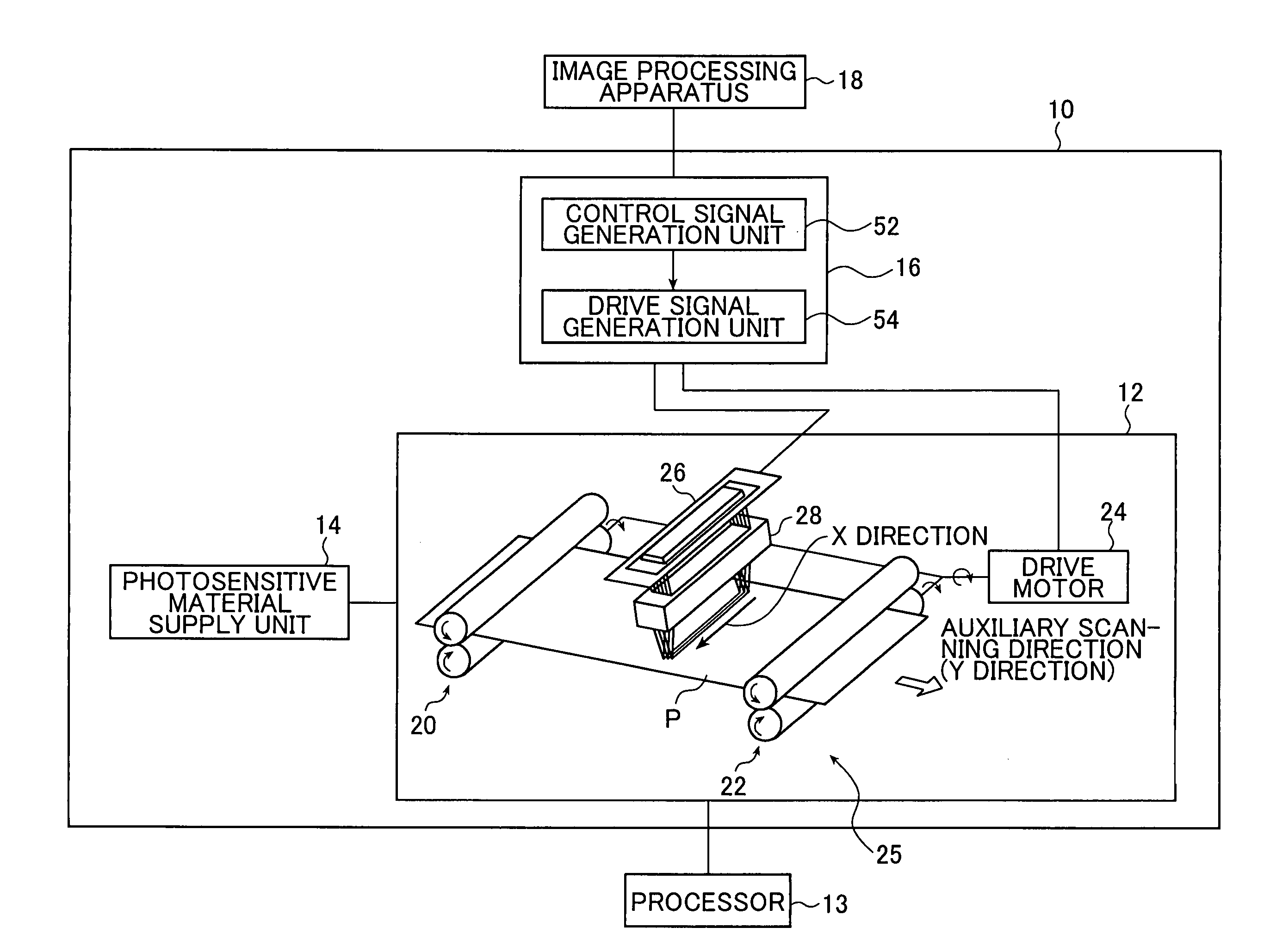
[0075]FIG. 1 is a construction diagram of a color printer 10 as an example of the image forming apparatus according to the present invention that forms an image by exposing a photosensitive material.

[0076]The printer 10 includes a head unit 12 that exposes and records a latent image on a photosensitive material P using a supplied image input signal, a photosensitive material supply unit 14 that transports and supplies the photosensitive material P to the head unit 12, and a signal processing unit 16 that generates a drive signal for driving the head unit 12 in order to expose and record an image on the photosensitive material P.

[0077]The signal processing unit 16 in the printer 10 is connected to an image processing apparatus 18 so that a post-image-processing signal subjected to imag...


PUM


Abstract

An image forming apparatus records an image on a photosensitive material by controlling a light emission amount from a plurality of light emission elements that each emit light in accordance with a supplied light emission control signal. The apparatus has a control signal generation unit and a first and second signal generation sections and a signal switching section. The control signal generation unit generates a first light amount control signal from a density modulation. The second signal generation section generates an ON / OFF control signal and a second light amount control signal as a pair of signals from a combination of a density modulation and an area modulation. The signal switching section generates a light emission control signal by performing signal switching between the first light amount control signal and the pair of the signals. The exposure by the light emission is overlaid. The second light amount control signal has short pulses having pulse widths shorter than a time constant of the initial rising stage of the light emission.

Description

BACKGROUND OF THE INVENTION[0001]The present invention relates to an image forming apparatus that exposes and records an image by controlling the light emission amount of each light emission element such as an organic electroluminescence element (hereinafter referred to as the “organic EL element”) using an image input signal, and an image forming method.[0002]A color print system for printing out an image of a photograph or the like records the image as a latent image by exposing a photosensitive material with modulated light and then prints out the image by processing and developing the latent image.[0003]Nowadays, various techniques are proposed with which in the color print system, organic EL elements are used as a light source for exposing the photosensitive material.[0004]Each organic EL element includes a cathode electrode forming an electron injection electrode, an anode electrode forming a hole injection electrode, and an organic layer that is a thin film arranged so as to ...

Claims


Application Information

Patent Timeline
Patent Type & Authority Patents(United States)
IPC IPC(8): B41J2/47G06K15/12H04N1/40
CPCG06K15/1209H04N1/40031G06K15/1247
Inventor ISHIBASHI, HIDEYASUHYUGA, HIROAKI
Owner FUJIFILM CORP
Why Eureka
Try Eureka