Semiconductor device for preventing defective filling of interconnection and cracking of insulating film

a technology of insulating film and defective filling, which is applied in the direction of semiconductor devices, semiconductor/solid-state device details, electrical equipment, etc., can solve the problems of difficult to achieve wire bonding unsuitability, copper interconnection is more corroded, and found technological limitations, so as to interconnections, prevent defective filling of buried conductors, and prevent cracking of inter-layer insulating films

Inactive Publication Date: 2007-11-27
SOCIONEXT INC
View PDF17 Cites 40 Cited by
  • Summary
  • Abstract
  • Description
  • Claims
  • Application Information

AI Technical Summary

Benefits of technology

[0018]An object of the present invention is to provide a semiconductor device having a structure that a conductor is buried in a hole-shaped pattern or a groove-shaped pattern formed in an insulating film and a method for fabricating the same, which can prevent the defective filling of the conductor and cracking of the insulating film due to the defective filling.
[0024]As described above, according to the present invention, in the semiconductor device having the structure that conductors are filled in the hole-shaped pattern and the groove-shaped pattern formed in the insulating films, even when a difference is generated between a finished size of the hole-shaped pattern and a finished size of the groove-shaped patterns, the defective filling of the buried conductor and the interconnections can be prevented. The defective filling of the buried conductor is prevented, whereby the cracking of the inter-layer insulating film can be prevented. Steps on the buried conductor plug can be reduced, so that the step cannot be influential on the upper interconnection layers and insulating layers. Accordingly, defective contact with the upper interconnection layer and the problems taking place in forming films can be prevented, and resultantly the semiconductor device can have high water resistance and high interconnection reliability.

Problems solved by technology

However, this has found technological limitation as the generations advance.
On the other hand, the copper interconnection is more corrosive than the conventionally used aluminum interconnection and is difficult for wire bonding unsuitably as an uppermost interconnection layer.
However, it has been found that the inductor including the aluminum interconnection layer has new problems which has not taken place in inductors formed of only copper interconnection layers.
The defective filling of the contact plugs causes poor. coverage of the barrier metal layer or the aluminum film in forming the upper interconnection layer formed thereon, the transfer of steps onto the surface of the interconnection layer formed thereon, etc.
Defective formation of the upper interconnection layer causes electrically weak parts in the connections between the contact plug and the interconnection.
Cracks in the inter-layer insulating film are a cause of inducing diffusion of copper from the lower interconnection layer.
Copper, which is easily diffused into silicon oxide film at certain temperatures, is a cause of lowering the breakdown voltage between the interconnections when the interconnection of a different potential is present in its neighborhood.
The copper is exposed in the interface at the cracks, which is a cause of poor electromigration immunity when excessive current flows.
However, the same problems take place in forming structures using the groove-shaped via patterns.
For example, in the case that the groove-shaped via patterns are used in a guard ring (also called as a seal ring) for protecting the device from water from the environments, etc., the above-described defect is a cause of degrading the moisture resistance.
Especially, the guard ring for a redundant circuit, which encloses a fuse region, cracks very influentially occur inside the chips.

Method used


Image

  • Semiconductor device for preventing defective filling of interconnection and cracking of insulating film
  • Semiconductor device for preventing defective filling of interconnection and cracking of insulating film
  • Semiconductor device for preventing defective filling of interconnection and cracking of insulating film

Examples


first embodiment

A FIRST EMBODIMENT

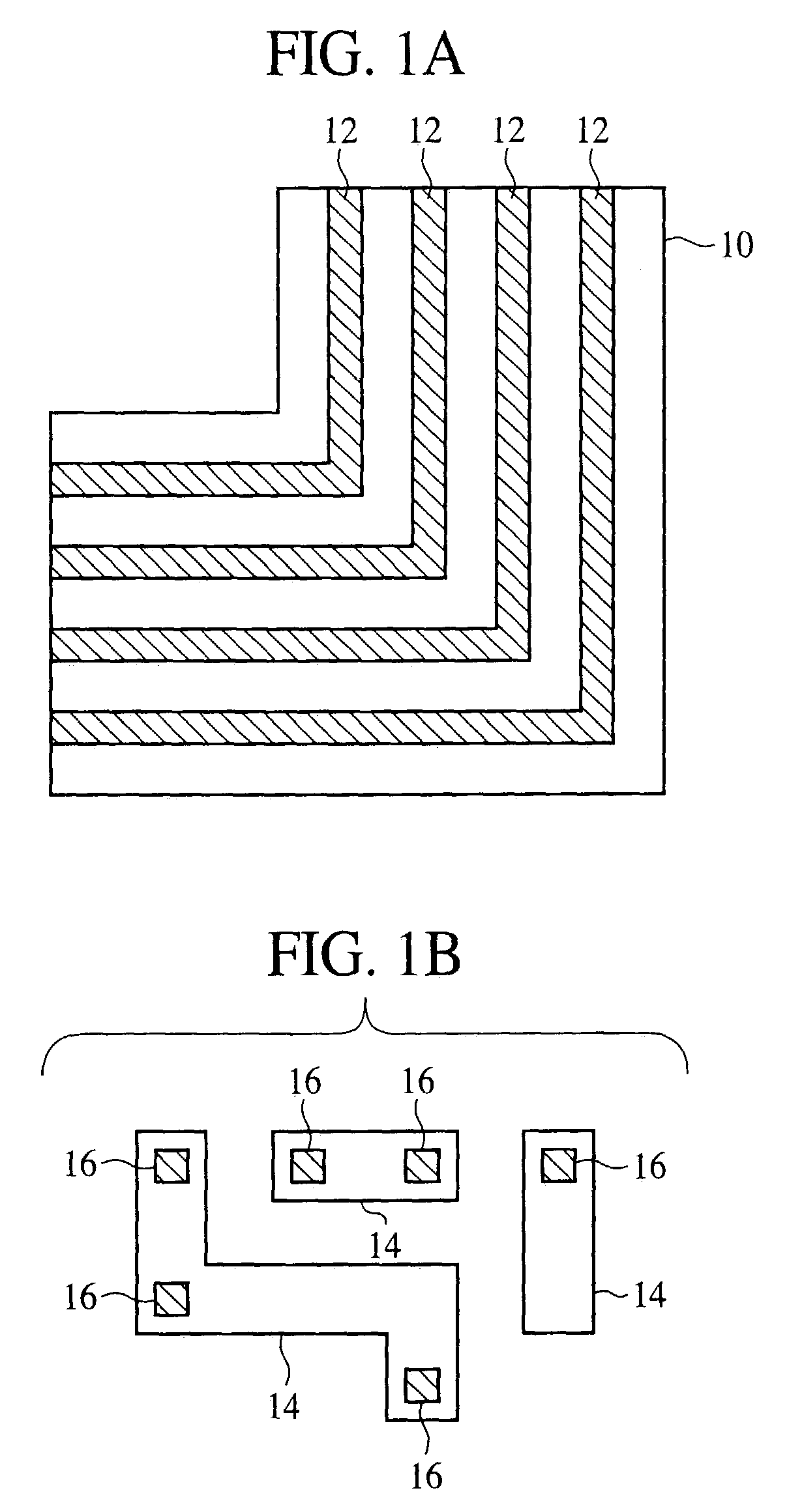
[0069]The semiconductor device and the method for fabricating the same according to a first embodiment of the present invention will be explained with reference to FIGS. 4A-4B, 5, 6, 7A-7C, 8A-8C, 9A-9B, 10A-10B, 11A-11B, 12A-12B, 13A-13B, and 14.

[0070]FIGS. 4A and 4B are plan views of a design structure of the semiconductor device according to the present embodiment. FIGS. 5 and 6 are diagrammatic sectional views of the semiconductor device according to the present embodiment, which show the structure. FIGS. 7A to 14 are sectional views of the semiconductor device according to the present embodiment in the steps of the method for fabricating the same, which show the method.

[0071]First, the structure of the semiconductor device according to the present embodiment will be explained with reference to FIGS. 4A to 6. FIG. 4A is a partial plan view of a design structure of the inner circuit region of the semiconductor device according to the present embodiment. FIG. 4B ...

second embodiment

A SECOND EMBODIMENT

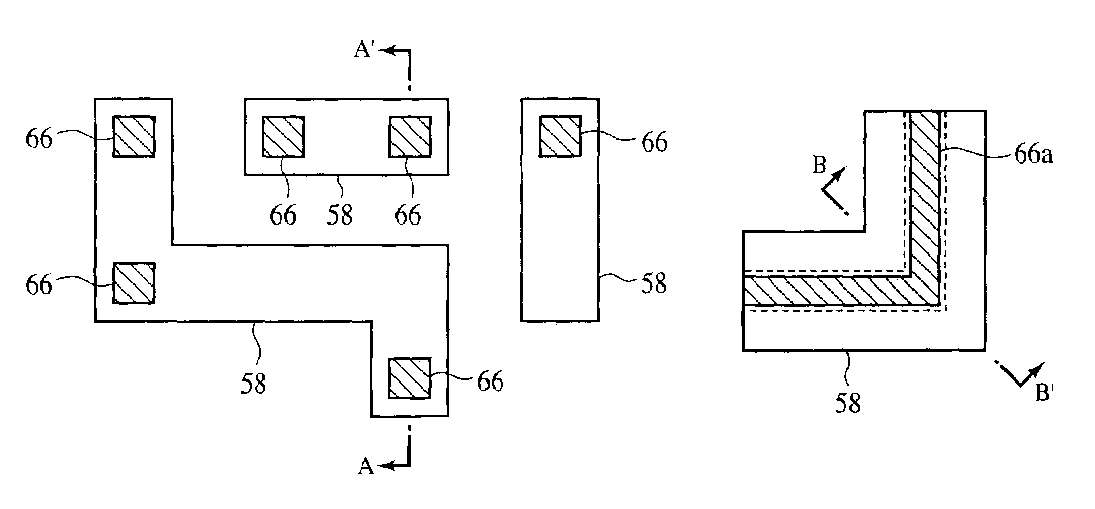
[0125]The semiconductor device and the method for fabricating the same according to a second embodiment of the present invention will be explained with reference to FIGS. 15 and 16. The same members of the present embodiment as those of the semiconductor device and the method for fabricating the same according to the first embodiment are represented by the same reference numbers not to repeat or to simplify their explanation.

[0126]FIG. 15 is a plan view of a design structure of the semiconductor device according to the present embodiment. FIG. 16 is a plan view of a design structure of the semiconductor device according to a modification of the present embodiment.

[0127]The semiconductor device and the method for fabricating the same according to the present embodiment is the same as the semiconductor device and the method for fabricating the same according to the first embodiment except that a plane design of a groove-shaped via-hole in a groove-shaped via pattern...

third embodiment

A THIRD EMBODIMENT

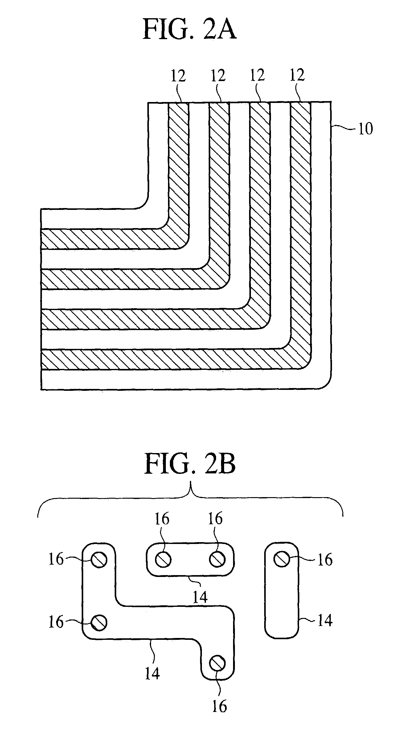
[0136]The semiconductor device and the method for fabricating the same according to a third embodiment of the present invention will be explained with reference to FIG. 17. The same members of the present embodiment as those of the semiconductor device and the method for fabricating the same according to the first and the second embodiments shown in FIGS. 4A-16 are represented by the same reference numbers not to repeat or to simplify their explanation.

[0137]FIG. 17 is a plan view of the design structure of the semiconductor device according to the present embodiment.

[0138]The semiconductor device and the method for fabricating the same according to the present embodiment is the same as the semiconductor device and the method for fabricating the same according to the first and the second embodiments except that the plane design of a groove-shaped via-hole in a groove-shaped via pattern forming region is different from that of the latter.

[0139]In the semiconductor d...


PUM


Abstract

The semiconductor device has insulating films 40, 42 formed over a substrate 10; an interconnection 58 buried in at least a surface side of the insulating films 40, 42; insulating films 60, 62 formed on the insulating film 42 and including a hole-shaped via-hole 60 and a groove-shaped via-hole 66a having a pattern bent at a right angle; and buried conductors 70, 72a buried in the hole-shaped via-hole 60 and the groove-shaped via-hole 66a . A groove-shaped via-hole 66a is formed to have a width which is smaller than a width of the hole-shaped via-hole 66. Defective filling of the buried conductor and the cracking of the inter-layer insulating film can be prevented. Steps on the conductor plug can be reduced. Accordingly, defective contact with the upper interconnection layer and the problems taking place in forming films can be prevented.

Description

CROSS-REFERENCE TO RELATED APPLICATIONS[0001]This application is based upon and claims the benefit of priority from the prior Japanese Patent Application No. 2002-223343, filed in Jul. 31, 2002, the entire contents of which are incorporated herein by reference.BACKGROUND OF THE INVENTION[0002]The present invention relates to a semiconductor device, more specifically a semiconductor device having a conductor buried in a hole-shaped pattern or a groove-shaped pattern formed in an insulating film, and a method for fabricating the semiconductor device.[0003]As semiconductor devices are larger-scaled and higher integrated, the design rules of interconnections are more shrunk with generations. Conventionally, interconnection layer has been formed by depositing and patterning the interconnection material by lithography and dry etching. However, this has found technological limitation as the generations advance. As a new process for forming interconnection layer, which takes the place of th...

Claims


Application Information

Patent Timeline
Patent Type & Authority Patents(United States)
IPC IPC(8): H01L27/04H01L23/48H01L23/52H01L23/522H01L23/532H01L21/768H01L21/822
CPCH01L23/522H01L29/0619H01L23/5329H01L23/585H01L23/485H01L29/0611H01L23/528H01L29/0607H01L23/5226H01L23/562H01L23/53228H01L23/53204H01L23/481H01L23/58H01L23/5227H01L23/53295H01L2924/0002H01L2924/00H01L27/04H01L21/76804H01L21/76843H01L21/76877H01L23/5283H01L23/53223H01L23/53266
Inventor WATANABE, KENICHI
Owner SOCIONEXT INC
Why Eureka
Try Eureka