Light-emitting apparatus and method of manufacturing the same

Inactive Publication Date: 2007-11-27
SEMICON ENERGY LAB CO LTD
View PDF29 Cites 21 Cited by
  • Summary
  • Abstract
  • Description
  • Claims
  • Application Information

AI Technical Summary

Benefits of technology

[0016]Therefore, the present invention has been made with the foregoing in mind, and it is an object of the present invention to provide a light-emitting d

Problems solved by technology

Furthermore, when the insulating surface under the first electrode is not flat and has foreign matters and unevenness with a thickness almost equal to or larger than that of the first electrode, the first electrode is not for

Method used


Image

  • Light-emitting apparatus and method of manufacturing the same
  • Light-emitting apparatus and method of manufacturing the same
  • Light-emitting apparatus and method of manufacturing the same

Examples


embodiment 1

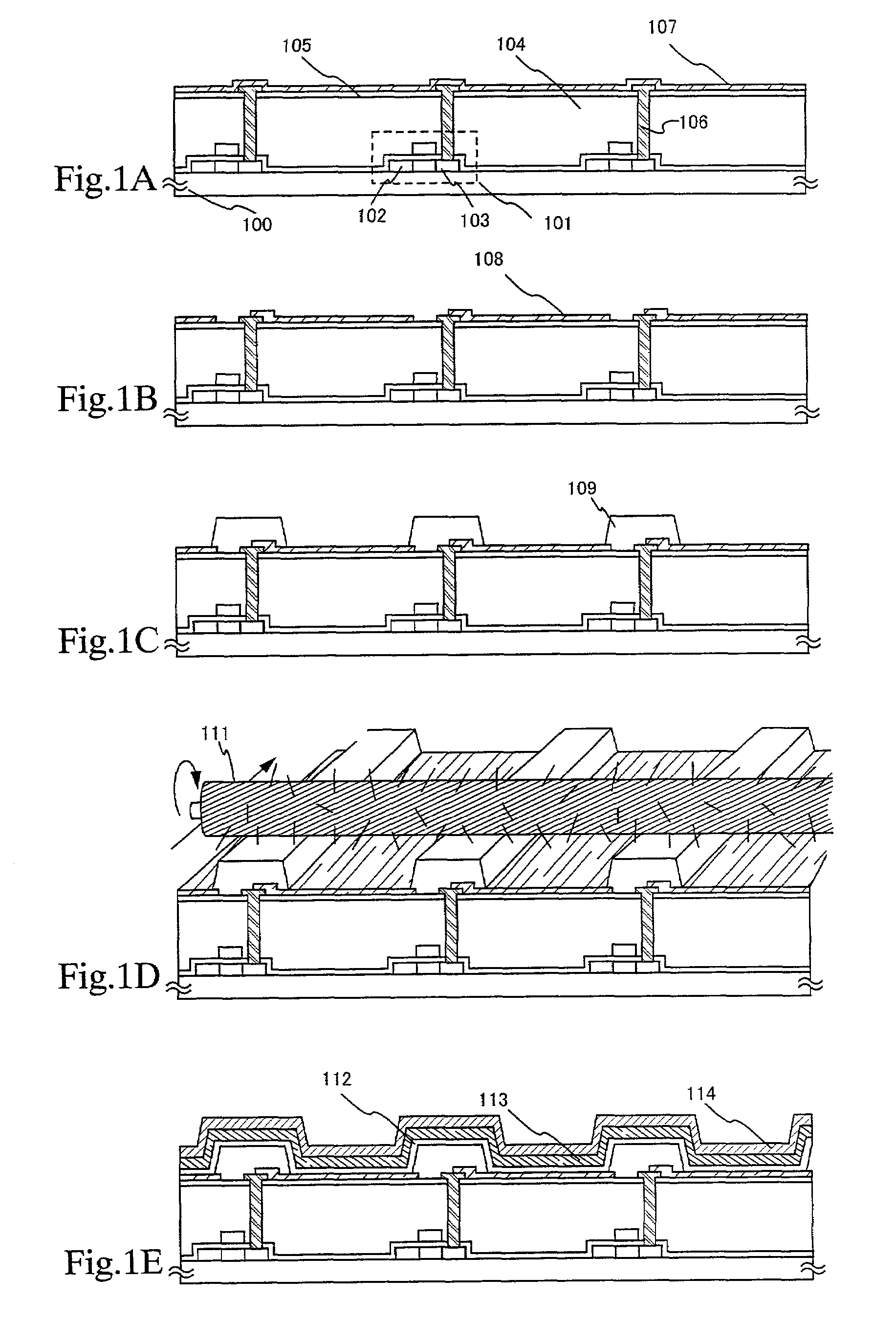
[0068]In this embodiment, the light-emitting element formed by using the present invention is explained. Described next is an example of a method of manufacturing, at the same time on the same substrate, TFTs for a pixel portion having a light-emitting element of the present invention and TFTs (an n-channel TFT and a p-channel TFT) for a driving circuit that is provided in the periphery of the pixel portion. The description will be given with reference to FIGS. 3A to 6C.

[0069]First, as shown in FIG. 3A, this embodiment uses a substrate 900 made of barium borosilicate glass, typically Corning #7059 glass and #1737 glass (products of Corning Incorporated), or alumino borosilicate glass. No limitation is put to the material of the substrate 900 as long as it is light-transmissive, and a quartz substrate may be used. A plastic substrate may also be used if it can withstand heat at the process temperature of this embodiment.

[0070]Next, a base film 901 is formed on the substrate 900 from ...

embodiment 2

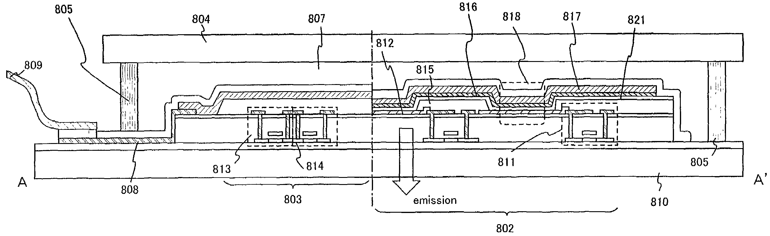
[0117]In Embodiment 1, the first electrode is formed of Mg—Ag, an Al—Li alloy film, or a film formed by co-deposition of an element belonging to Group I or II of the periodic table and aluminum, and the second electrode is formed of a transparent conductive film material, whereby a light-emitting device emitting light to the opposite side of the substrate 100 can be produced.

embodiment 3

[0118]The processes are conducted in the same way as in Embodiment 1 until the second interlayer insulating film 935 is formed. Then, the second interlayer insulating film 935 is subjected to a plasma treatment, in place of forming the insulating film 936 in Embodiment 1, whereby the surface of the second interlayer insulating film 935 is modified. This method will be described with reference to FIG. 7.

[0119]The second interlayer insulating film 935 is subjected to a plasma treatment in one kind or a plurality of kinds of gases selected from the group consisting of hydrogen, nitrogen, hydrocarbon, halocarbon, hydrogen fluoride, and noble gas (Ar, He, Ne, etc.), whereby a new coating film is formed on the surface of the second interlayer insulating film 953, or the kind of a functional group present on the surface is changed. As a result, the surface of the second interlayer insulating film 935 can be modified. On the surface of the second interlayer insulating film 935, a densified ...


PUM


Abstract

A light-emitting apparatus of the present invention includes: a first electrode formed on an insulating surface; a first insulating layer covering an end portion of the first electrode and having a tapered edge; a second insulating layer formed on the first electrode and the first insulating layer and formed of one kind or a plurality of kinds selected from the group consisting of silicon oxide, silicon nitride, and silicon oxynitride; an organic compound layer formed on the second insulating layer; and a second electrode formed on the organic compound layer.

Description

BACKGROUND OF THE INVENTION[0001]1. Field of the Invention[0002]The present invention relates to a light-emitting device using a light-emitting element which has a film (hereinafter, referred to as an “organic compound layer”) containing an organic compound that emits light through fluorescence and phosphorescence by applying an electric field, and a method of manufacturing the same.[0003]2. Description of the Related Art[0004]A light-emitting element using an organic compound as an illuminant has characteristics such as thinness and light-weight, high response, and driving at a D.C. current and a low voltage. Thus, such light-emitting element is expected to be applied to a next-generation flat panel display. In particular, a display device with light-emitting elements arranged in matrix is considered to have the advantages of a wide viewing angle and excellent visibility, compared with a conventional liquid crystal display device.[0005]According to a light-emitting mechanism of a l...

Claims


Application Information

Patent Timeline
IPC IPC(8): H01L51/52H01L27/32
CPCH01L27/1214H01L51/5253H01L51/5206H01L27/3246H01L29/4908H01L29/42384H01L27/1259H10K59/122H10K50/81H10K50/844H10K59/1201
Inventor SAKAKURA, MASAYUKIYAMAZAKI, SHUNPEI
Owner SEMICON ENERGY LAB CO LTD
Why Eureka
Try Eureka