Flash memory device and method of fabricating the same

a flash memory and memory device technology, applied in the field of flash memory devices, can solve the problems of reducing the performance of a product, affecting the operation of mlc cells, and reducing the efficiency of mlc cells, so as to reduce the interference effect of neighboring cells and reduce the threshold voltag

Active Publication Date: 2007-12-11
SK HYNIX INC
View PDF8 Cites 0 Cited by
  • Summary
  • Abstract
  • Description
  • Claims
  • Application Information

AI Technical Summary

Benefits of technology

[0014]Accordingly, the present invention relates to providing flash memory devices and method of fabricating the same, wherein a shift in a threshold voltage due to the interference effect of neighboring cells can be reduced.

Problems solved by technology

However, the technology innovations and improvements needed to enable such device shrinkage are becoming more and more difficult to achieve in part due to the limits associated with patterning technology and equipment.
If the range for one level or sensing margin is too finely controlled, however, the performance of a product can be degraded.
However, a threshold voltage value (dVt) that varies due to neighboring cells in a word line direction is 0.3 to 0.5 V. This makes it difficult to implement a MLC cell.

Method used


Image

  • Flash memory device and method of fabricating the same
  • Flash memory device and method of fabricating the same
  • Flash memory device and method of fabricating the same

Examples


Embodiment Construction

[0033]Now, the preferred embodiments according to the present invention will be described with reference to the accompanying drawings. Since preferred embodiments are provided for the purpose that the ordinary skilled in the art are able to understand the present invention, they may be modified in various manners and the scope of the present invention is not limited by the preferred embodiments.

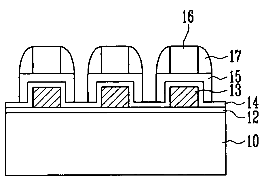
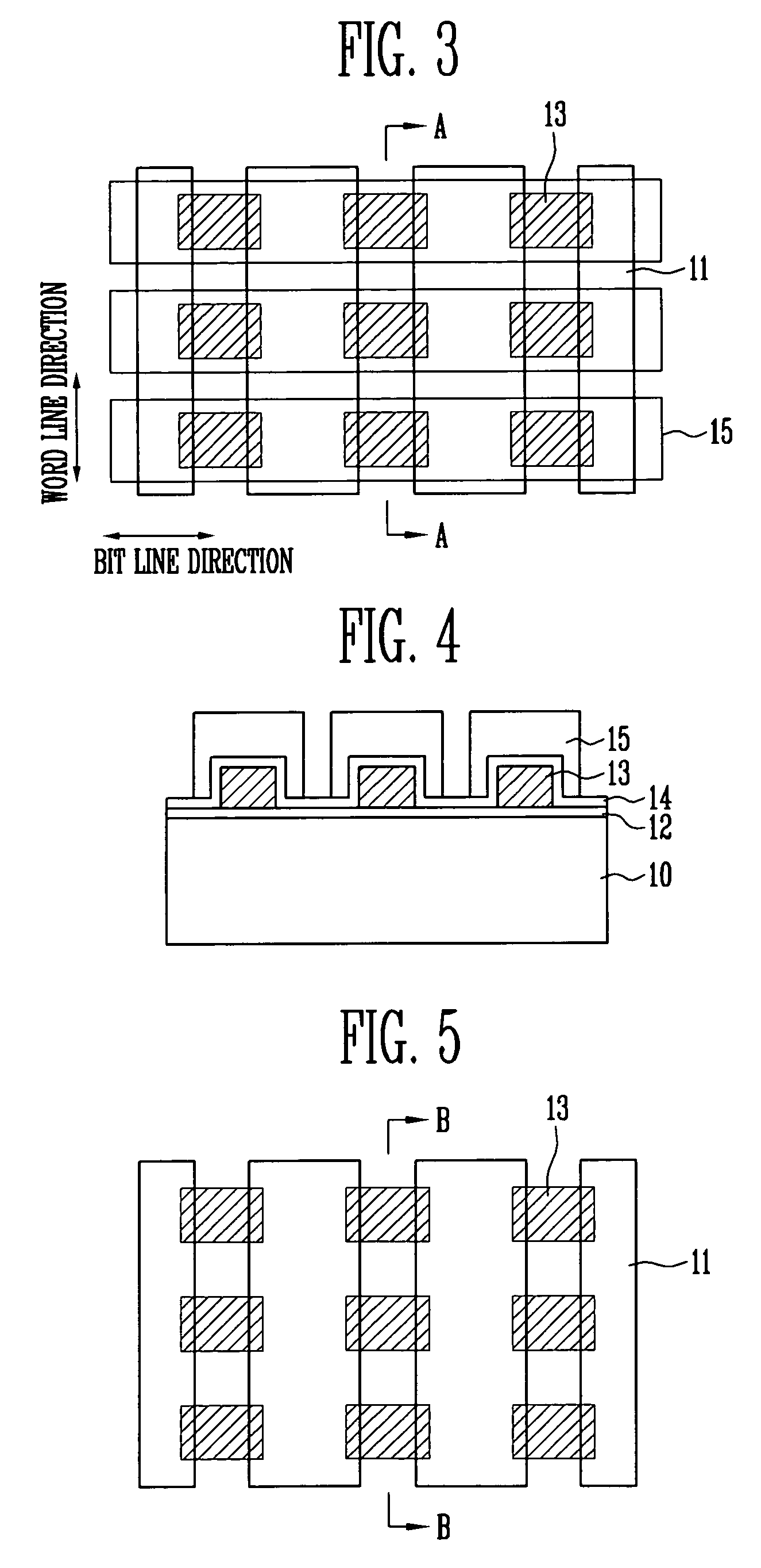
[0034]FIG. 3 is a plan view showing a flash memory device according to an embodiment of the present invention. FIG. 4 is a cross-sectional view of the flash memory device taken along line A-A in FIG. 3.

[0035]Referring to FIGS. 3 and 4, isolation films 11 of a stripe pattern, which are arranged in a word line direction, divide a semiconductor substrate 10 into an active region and a field region. A tunnel dielectric film 12 is formed along a surface of the semiconductor substrate 10 in which the isolation films 11 are formed. A plurality of floating gates 13, which are separated on a cell basi...


PUM


Abstract

A flash memory device includes control gates that are formed to completely surround the top and sides of floating gates. The control gates are located between the floating gates that are adjacent in the word line direction as well as the floating gates that are adjacent in the bit line direction. The present flash memory device reduces a shift in a threshold voltage resulting from interference among floating gates and increases an overlapping area of the floating gate and the control gates. Thus, there is an effect in that the coupling ratio can be increased.

Description

CROSS-REFERENCES TO RELATED APPLICATIONS[0001]The present application claims priority to Korean Patent Application No. 10-2005-0039859, filed May 12, 2005, which is incorporated by reference.BACKGROUND OF THE INVENTION[0002]The present invention relates to flash memory devices, and more specifically, to flash memory devices and method of fabricating the same, wherein interference among floating gates can be reduced and the coupling ratio can be enhanced.[0003]The size of flash memory cells preferably needs to be made smaller and smaller. However, the technology innovations and improvements needed to enable such device shrinkage are becoming more and more difficult to achieve in part due to the limits associated with patterning technology and equipment.[0004]As a result, much research has been done on a multi-bit cell technology, in which a plurality of data can be stored in one memory cell. This type of a memory cell is called a “multi-level cell (MLC)”.[0005]A MLC generally has two...

Claims


Application Information

Patent Timeline
Patent Type & Authority Patents(United States)
IPC IPC(8): H01L21/336
CPCH01L27/11521H01L27/115H10B69/00H10B41/30H10B99/00
Inventor KIM, KI SEOG
Owner SK HYNIX INC
Why Eureka
Try Eureka