
Fluorinated graphene passivated AlGaN/GaN-based HEMT device and manufacturing method

a fluorinated graphene and hemt technology, applied in the field of microelectronic and solid-state electronic, can solve the problems of greatly reduced output performance, and achieve the effects of low additional effect on threshold voltage, good isolation performance, and small physical thickness

Active Publication Date: 2020-09-08
SHANGHAI INST OF MICROSYSTEM & INFORMATION TECH CHINESE ACAD OF SCI
View PDF7 Cites 0 Cited by
  • Summary
  • Abstract
  • Description
  • Claims
  • Application Information

AI Technical Summary

Benefits of technology

This patent describes a new method and structure for a type of semiconductor device called an AlGaN / GaN HEMT. This method uses a high-k material and a single-layer of graphene that is protected by fluoride ions and acts as a replacement for a traditional nitride passivation layer. Compared to traditional methods, this new method has several advantages including smaller physical thickness and low additional effects on threshold voltage. The graphene also acts as a good isolation barrier, preventing surface oxidation and traps that can affect the performance of the device. The method is simple and has wide application potential in microelectronics and solid-state electronics. Overall, this patent provides a new and effective way to design and manufacture AlGaN / GaN HEMT devices.

Problems solved by technology

If the thickness of the n-AlxGal-xAs control layer is large and the doping concentration is high, 2-DEG exists when Vg=0, and the device is a depletion device; contrarily, the device is an enhancement device (when Vg=0, Schottky depletion layer extends to the inside of an i-GaAs layer); and however, if the thickness of the layer is too large and the doping concentration is too high, 2-DEG cannot be depleted during working and leakage resistance associated with S-D will appear.
However, due to the existence of surface electron traps, unpassivated AlGaN / GaN HEMT usually presents serious current collapse phenomena and the output performance is greatly reduced.

Method used


Image

  • Fluorinated graphene passivated AlGaN/GaN-based HEMT device and manufacturing method
  • Fluorinated graphene passivated AlGaN/GaN-based HEMT device and manufacturing method
  • Fluorinated graphene passivated AlGaN/GaN-based HEMT device and manufacturing method

Examples


Embodiment Construction

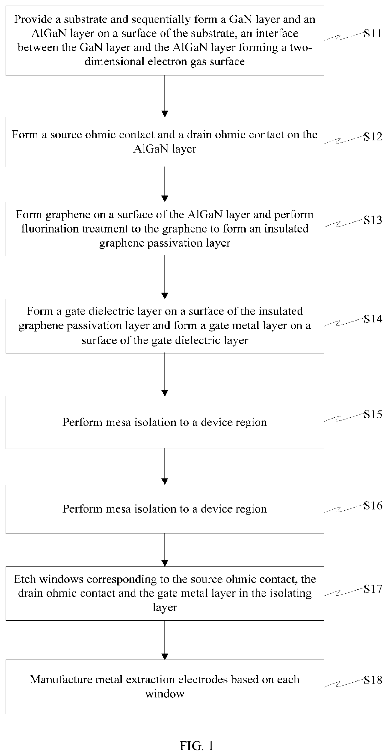
[0034]The implementation modes of the present invention will be described below through specific examples. One skilled in the art can easily understand other advantages and effects of the present invention according to content disclosed in the description. The present invention may also be implemented or applied through other different specific implementation modes. Various modifications or variations may be made to all details in the description based on different points of view and applications without departing from the spirit of the present invention.

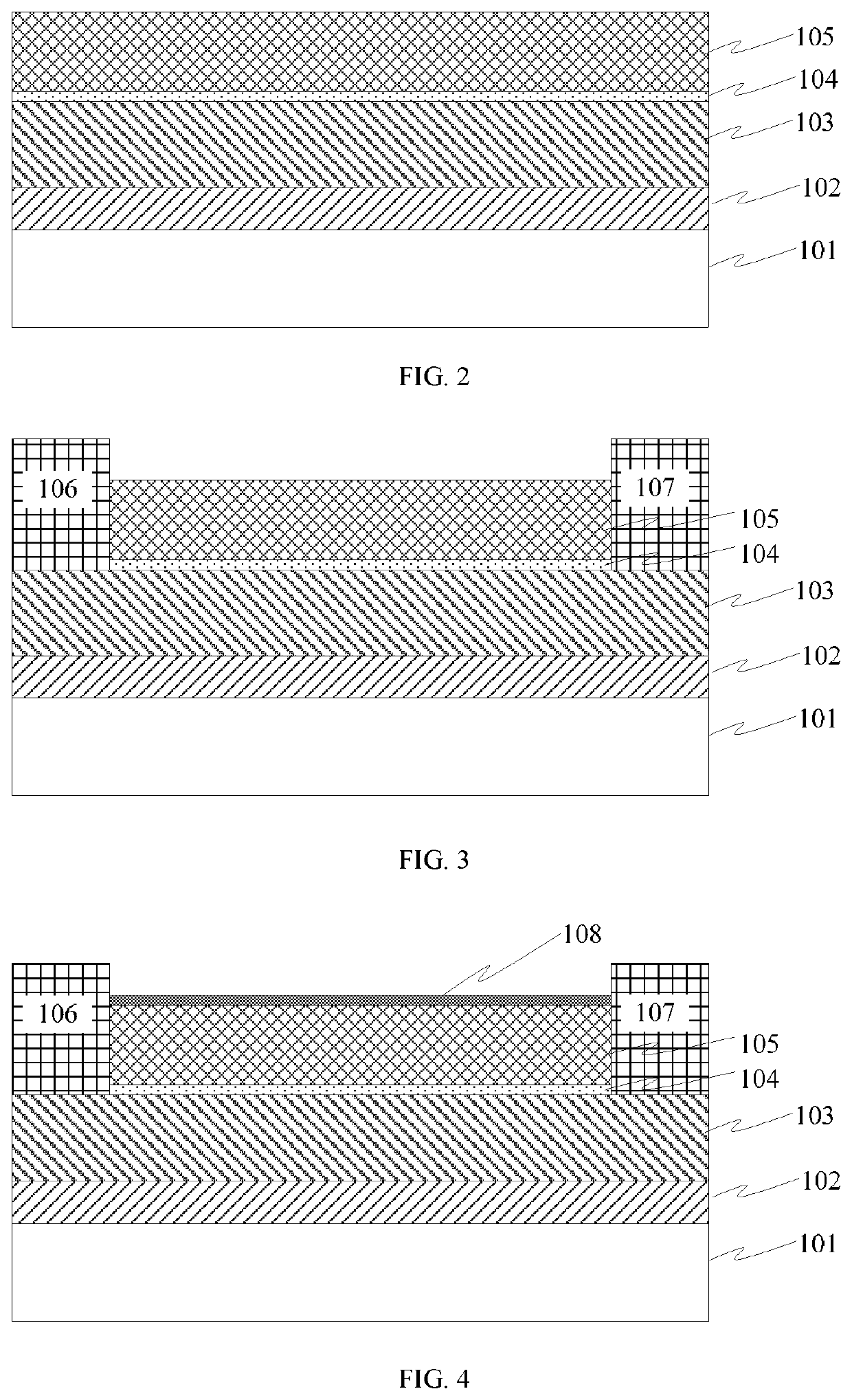
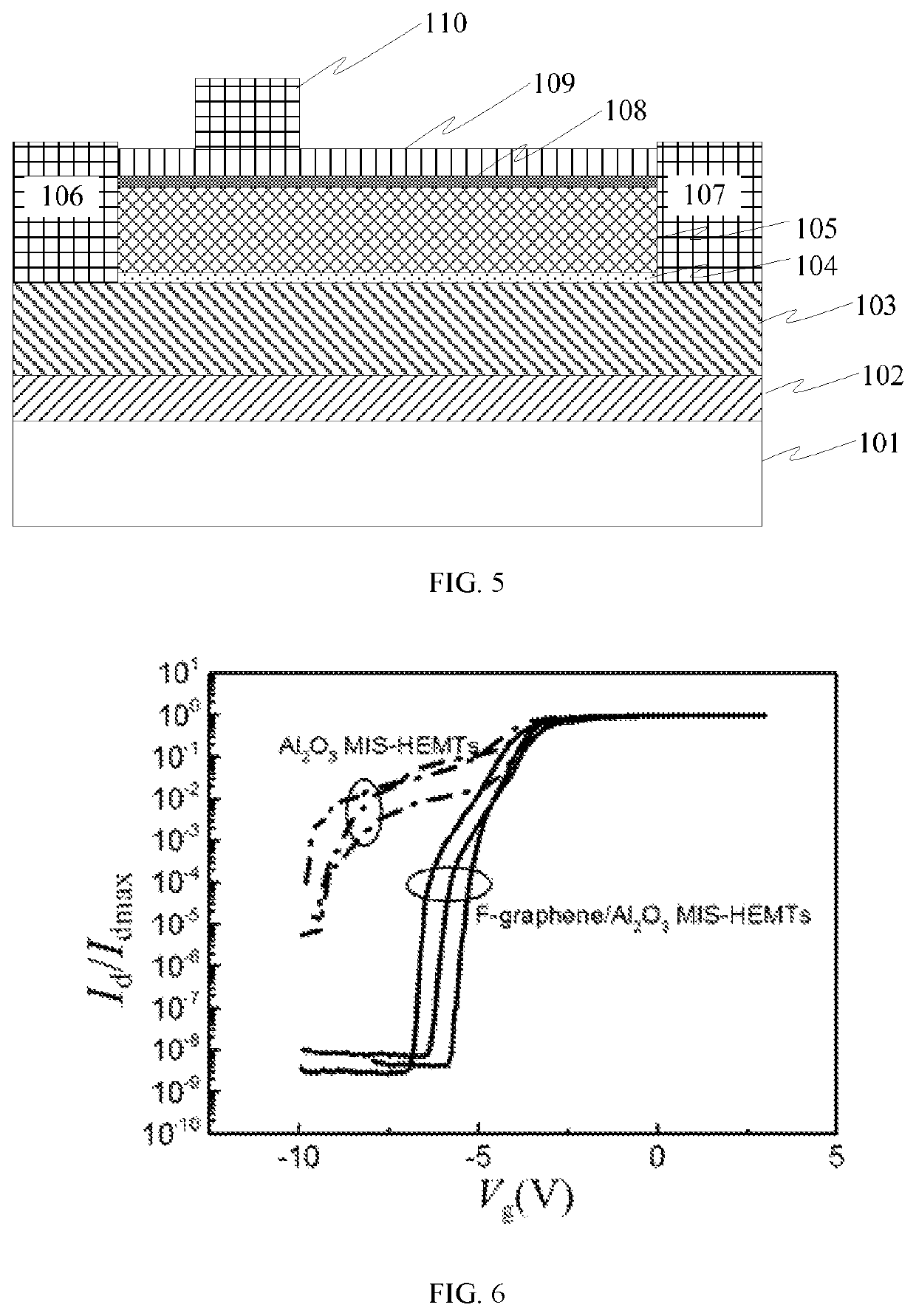
[0035]Please refer to FIG. 1 to FIG. 7. It needs to be stated that the drawings provided in the following embodiments are just used for schematically describing the basic concept of the present invention, thus only illustrate components only related to the present invention and are not drawn according to the numbers, shapes and sizes of components during actual implementation, the configuration, number and scale of each component du...


PUM

PropertyMeasurementUnit
thicknessaaaaaaaaaa
thicknessaaaaaaaaaa
thicknessaaaaaaaaaa

Abstract

An AlGaN / GaN HEMT based on fluorinated graphene passivation and a manufacturing method thereof. Monolayer graphene (108) is transferred to an AlGaN (104) surface, is treated by using fluoride ions and then is insulated to thereby replace a conventional nitride passivation layer. Then, a high-k material (109) is grown on the graphene (108), and the high-k material (109) and the graphene (108) are jointly used as a gate dielectric for preparing an AlGaN / GaN metal-insulator-semiconductor (MIS) HEMT. Compared with the traditional passivation structure, the graphene (108) has the advantages of small physical thickness (sub-nanometer scale) and low additional threshold voltage. The structure and the method are simple, the effect is remarkable and the application prospect in technical fields of microelectronics and solid-state electronics is wide.

Description

CROSS REFERENCE TO RELATED PATENT APPLICATION[0001]The present application is the US national stage of PCT / CN2016 / 075635 filed on Mar. 4, 2016, which claims the priority of the Chinese patent application No. CN2015107723843 filed on Nov. 12, 2015, which application is incorporated herein by reference.BACKGROUND OF THE PRESENT INVENTIONField of Invention[0002]The present invention belongs to technical field of microelectronic and solid-state electronic, and in particular relates to an AlGaN / GaN HEMT based on fluorinated graphene passivation and manufacturing method thereof.Description of Related Arts[0003]High Electron Mobility Transistor (HEMT) is a heterojunction-field effect transistor, which is also called as a Modulation-Doped Field Effect Transistor (MODFET), a 2-Dimensional Electron Gas Field Effect Transistor (2-DEGFET), Selectively-Doped Heterojunction Transistor (SDHT), etc. This device and integrated circuits thereof can work at an ultrahigh frequency (millimeter wave) and...

Claims


Application Information

Patent Timeline
Patent Type & Authority Patents(United States)
IPC IPC(8): H01L21/02H01L21/338H01L29/40H01L29/51H01L29/778H01L29/205H01L29/66H01L29/20
CPCH01L29/401H01L29/7787H01L29/205H01L29/7786H01L29/408H01L29/513H01L29/66462H01L29/2003H01L29/517H01L29/0688H01L2229/00
Inventor CHENG, XINHONGSHEN, LINGYANWANG, ZHONGJIANCAO, DUOZHENG, LIWANG, QIANZHANG, DONGLIANGLI, JINGJIEYU, YUEHUI
Owner SHANGHAI INST OF MICROSYSTEM & INFORMATION TECH CHINESE ACAD OF SCI
Learn More