Methods and tangible objects employing machine readable data in photo-reactive materials

a technology of photo-reactive materials and machine readable data, applied in the field of methods and tangible objects employing machine readable data in photo-reactive materials, can solve the problems of many enterprises suffering from fraudulent product substitution, chips with lower speed ratings, and failure to meet the more demanding spec under some extreme operating conditions. , to achieve the effect of chip inspection

Inactive Publication Date: 2007-12-25
DIGIMARC CORP
View PDF14 Cites 52 Cited by
  • Summary
  • Abstract
  • Description
  • Claims
  • Application Information

AI Technical Summary

Problems solved by technology

Many enterprises suffer by such fraudulent product substitution.
Commonly, chips with lower speed ratings are produced on the same fabrication lines as chips with top speed ratings but, during post-fab testing, fail to meet the more demanding spec under some extreme of operating conditions (e.g. at stressful ambient conditions, marginal power supply potentials, etc.).
This testing is complex, costly, and time-consuming, but is viewed as necessary in order to assure the quality of the computer company's products.
While this electrical-encoding approach obviates the need for the purchaser to perform its own lengthy quality assurance testing, other drawbacks persist.
So doing exposes the chip to potential static damage, thus requiring that this procedure be performed in a highly controlled environment by skilled personnel.
Moreover, this approach increases the semiconductor die size, and impacts the yield.
While an improvement in some respects over the fusible link approach, this latter technique has drawbacks of its own.
For example, the provision of the metal traces on or near the exterior of the package limits packaging options, and makes assembly of the package more complex.
But the “bandwidth” of such inconspicuous techniques is quite limited, commonly being restricted to a single valid / invalid determination.
Moreover, most such techniques are ill-suited for after-the-fact application to an article.

Method used


Image

  • Methods and tangible objects employing machine readable data in photo-reactive materials
  • Methods and tangible objects employing machine readable data in photo-reactive materials

Examples


Embodiment Construction

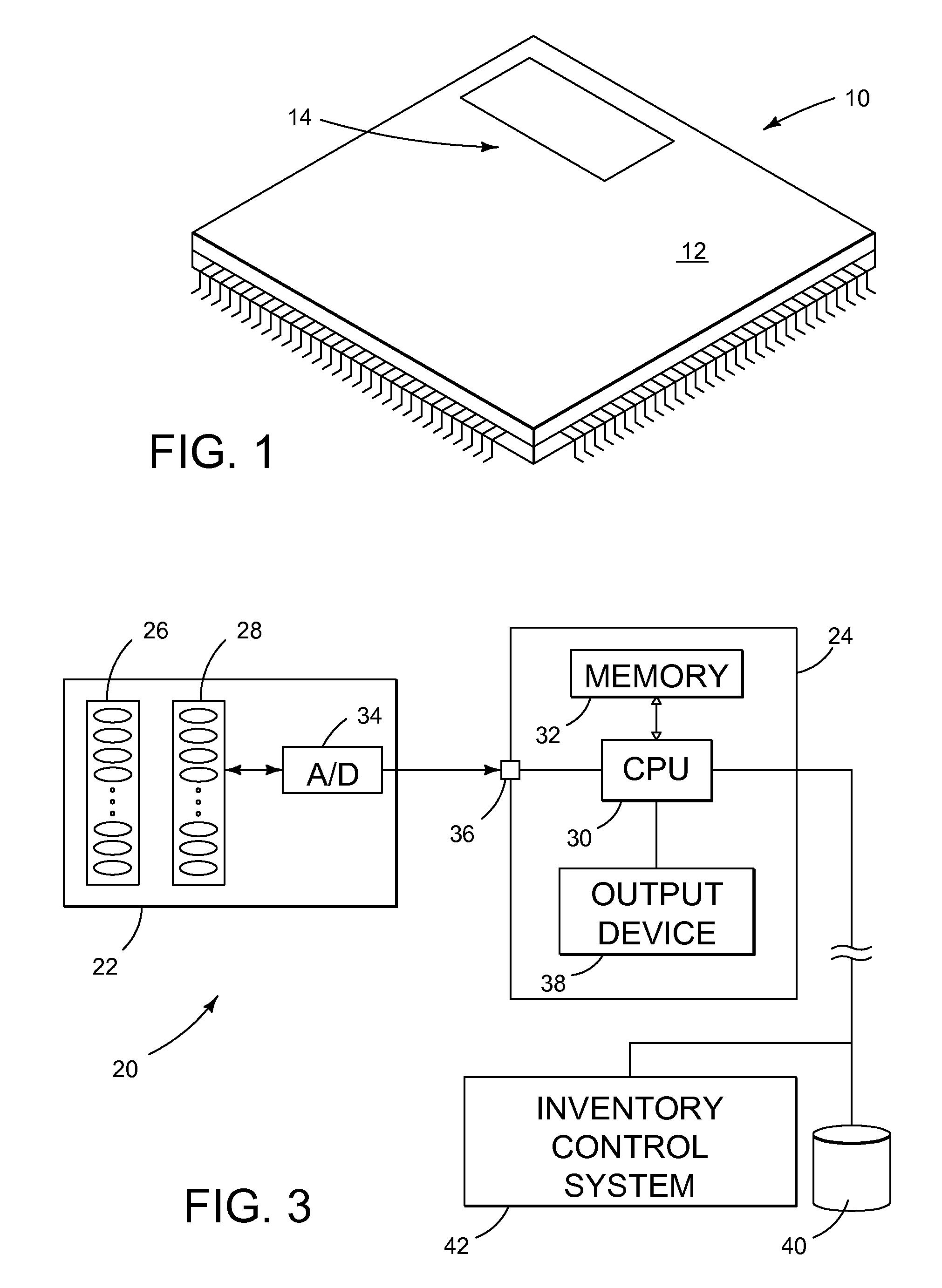
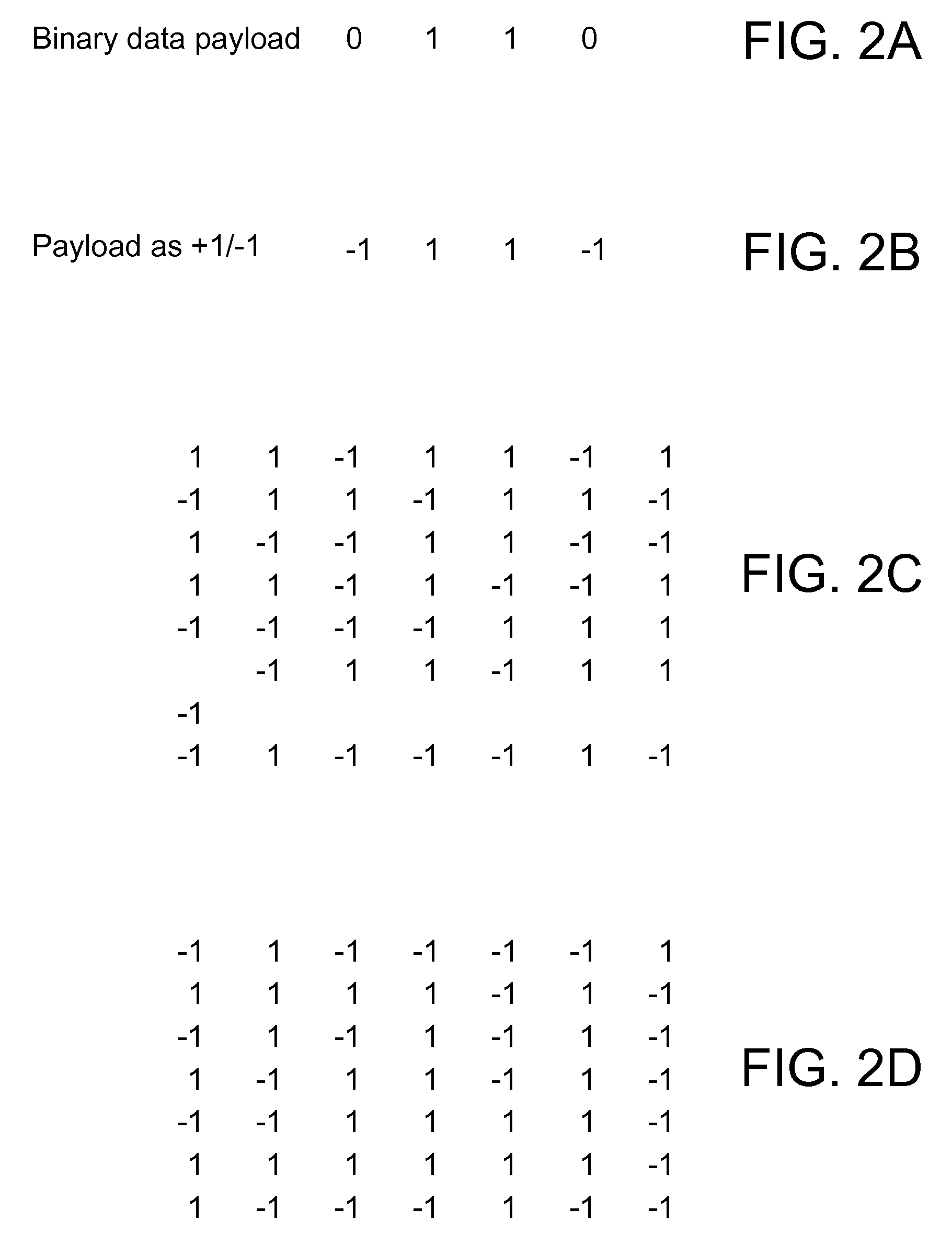
[0025]Referring to FIG. 1, an integrated circuit 10 includes an exterior housing, or package 12. The housing can be formed in numerous ways. One is by injection molding. Another is by known ceramic-shaping techniques. At some point prior to shipment, the surface micro-topology of an area 14 on the housing is shaped in a seemingly random manner. (The area 14 can span the entire housing, if desired.) In the preferred embodiments, the patterning is substantially uniform across its extent, and may look like pebbling, mottling, graininess, or roughness. Yet this seemingly random surface conveys plural-bit digital information.

[0026]In an illustrative production cycle, a semiconductor wafer is processed to form several integrated circuits. Testing is conducted to determine the speed rating (or other grade) of each circuit. (The testing can be done while all the circuits are still on the wafer, or after the wafer has been diced into dies, or after the dies have been packaged in a housing.) ...


PUM

PropertyMeasurementUnit
sizeaaaaaaaaaa
sizeaaaaaaaaaa
speed ratingsaaaaaaaaaa

Abstract

The present invention relates generally to steganography and data hiding. In one implementation we provide a method including: obtaining auxiliary data; providing a mask for a photo-reactive material, the mask corresponding at least in part to the auxiliary data; and exposing the material through the mask to steganographically impart the auxiliary data in the photo-reactive material. The auxiliary data is machine-readable from the exposed material. In another implementation the material is exposed through photolithographic illumination. Of course, other implementations are described and claimed as well.

Description

RELATED APPLICATION DATA[0001]This application is a continuation of U.S. patent application Ser. No. 11 / 456,809, filed Jul. 11, 2006, which is a continuation of application Ser. No. 11 / 106,186, filed Apr. 13, 2005 (now U.S. Pat. No. 7,076,084), which is a continuation of application Ser. No. 10 / 693,269, filed Oct. 23, 2003 (now U.S. Pat. No. 6,882,738), which is a continuation of application Ser. No. 09 / 151,492, filed Sep. 11, 1998 (now abandoned). This application is also related to application Ser. No. 08 / 438,159, filed May 8, 1995 (now U.S. Pat. No. 5,850,481), which is a continuation-in-part of application Ser. No. 08 / 327,426, filed Oct. 21, 1994 (now U.S. Pat. No. 5,768,426), which is a continuation-in-part of abandoned application Ser. No. 08 / 215,289, filed Mar. 17, 1994.[0002]The subject matter of this application is also related to that of the present assignee's other issued U.S. Pat. Nos. (5,636,292, 5,710,834, 5,721,788, 5,745,604, 5,748,763, 5,748,783, 5,768,426, and 5,80...

Claims


Application Information

Patent Timeline
Patent Type & Authority Patents(United States)
IPC IPC(8): H04K1/00G06T1/00G07C9/00G07D7/00G07D7/12G07F7/08G07F7/10G07F7/12G07F17/16G10L19/00G11B20/00H01L23/544H01L23/58H04B1/66H04N1/00H04N1/32H04N5/913
CPCG06K19/06009G06Q20/40145G06T1/0021G07C9/00079G07D7/0013G07D7/004G07F7/08G07F7/086G07F7/1008G07F7/1016G07F7/12G09F3/00G10L19/018G11B20/00086G11B20/00094G11B20/00166G11B20/00876G11B20/00884G11B20/00891H01L23/544H01L23/573H04B1/665H04N1/00005H04N1/00037H04N1/00079H04N1/00838H04N1/00846H04N1/32144H04N1/32208H04N1/32251H04N1/32288H04N5/913G06Q20/341H04N2201/328G06T2201/0052H01L2223/54486H04N1/32122H04N2005/91321H04N2005/91335H04N2201/3205H04N2201/3207H04N2201/3226H04N2201/3233H04N2201/327H04N2201/3271H01L2924/0002G07D7/0032G07C9/253H01L2924/00
Inventor DAVIS, BRUCE L.RHOADS, GEOFFREY B.
Owner DIGIMARC CORP
Why Eureka
Try Eureka