


Quick Research
Generate reliable direction feasibility study reports for your R&D in just a few steps.

Technical Q&A
Discover and master advanced knowledge NOW. Basics, ideas, possibilities, all at once.

Find Solutions
As an expert in R&D theories, this can generate solutions to your technical problems instantly.

Evaluate Feasibility
Analyze your overall solution with one click, know your potential R&D risks in advance.

Monitor Landscape
Get weekly tech updates, stay abreast of the latest tech innovations and key insights.
Solid-state image sensor device and driving method
- Summary
- Abstract
- Description
- Claims
- Application Information
AI Technical Summary
Benefits of technology
Problems solved by technology
Method used
Image

Examples
Embodiment Construction
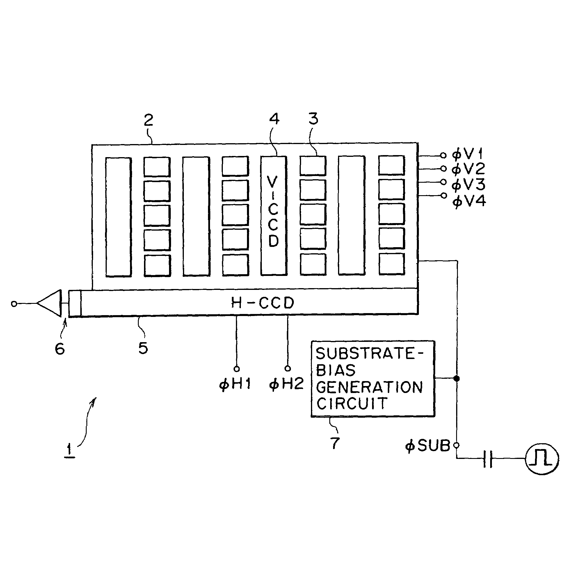
[0018]In the following, a solid-state image sensor device and its driving method according to the present invention will be explained referring to the drawings. FIG. 1 shows a schematic of an embodiment of a solid-state image sensor device according to the present invention.
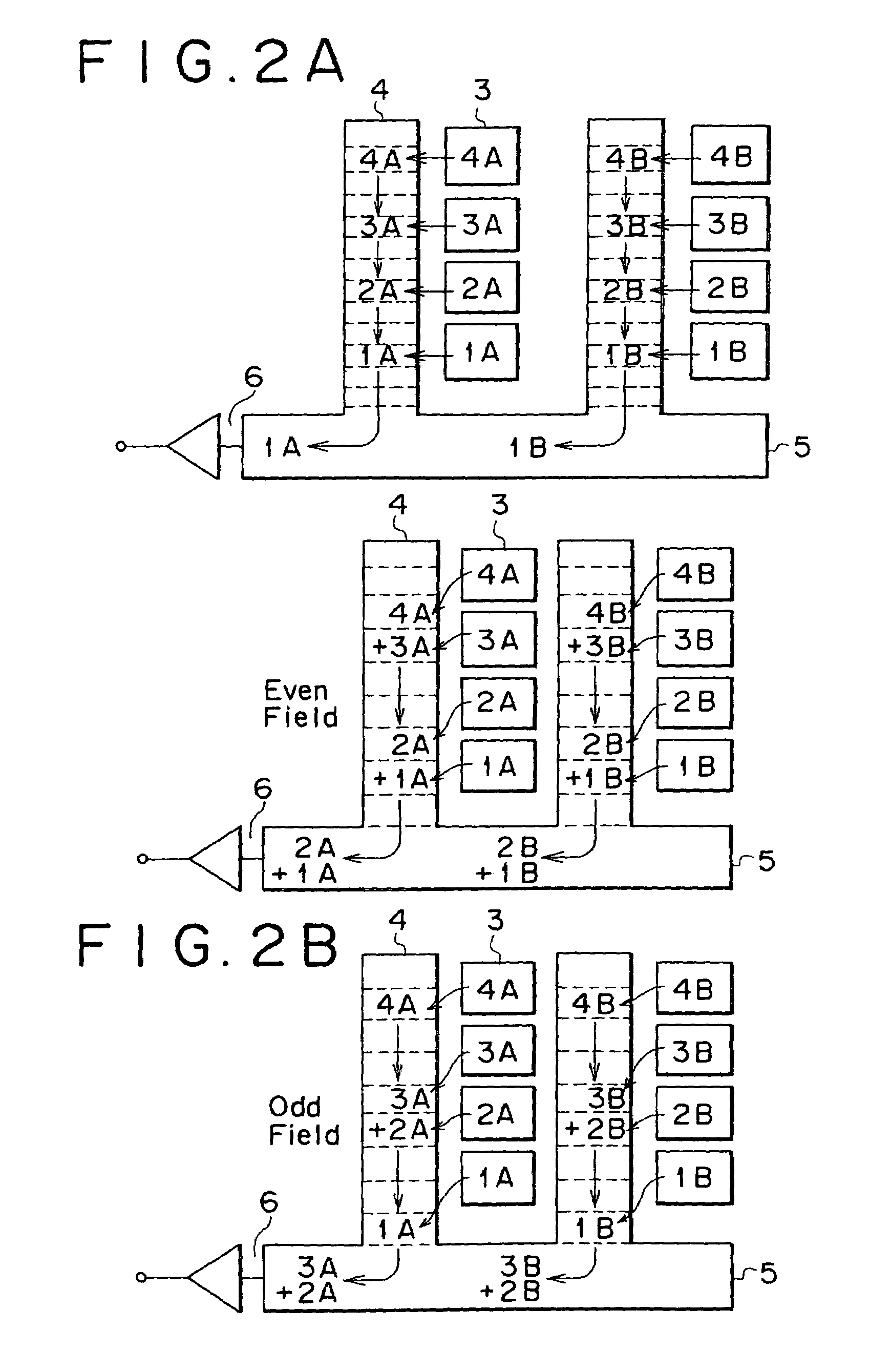
[0019]As shown in the figure, a solid-state image sensor device 1 in the present embodiment comprises an image sensing portion 2 in which photoelectric conversion is performed in unit of picture elements. The image sensing portion 2 is composed of a plurality of photodiodes 3 disposed two dimensionally in a matrix form in which an incident light is converted to a signal charge in unit of picture elements and accumulated in it, and a vertical transfer portion (V-CCD) 4 for transferring signal charges read out of each vertical column of the photodiodes 3 in the vertical direction. The V-CCD 4 takes charge of the operation corresponding to a vertical scanning and it is driven in the form of 4 phase-drive by vertical...
PUM
 Abstract
Description
Claims
Application Information
 - R&D Engineer
- R&D Manager
- IP Professional
- Industry Leading Data Capabilities
- Powerful AI technology
- Patent DNA Extraction
Browse by: Latest US Patents, China's latest patents, Technical Efficacy Thesaurus, Application Domain, Technology Topic, Popular Technical Reports.
© 2024 PatSnap. All rights reserved.Legal|Privacy policy|Modern Slavery Act Transparency Statement|Sitemap|About US| Contact US: help@patsnap.com