Interpolator based clock and data recovery (CDR) circuit with digitally programmable BW and tracking capability

a clock and data recovery circuit technology, applied in the field of high-speed encoded data communication, can solve the problems of limiting the tracking capability (or bandwidth) of the cdr circuit, affecting the speed of data transmission, so as to increase the bandwidth of the cdr, reduce the latency, and maintain the constant bandwidth

Active Publication Date: 2008-01-01
TEXAS INSTR INC
View PDF6 Cites 60 Cited by
  • Summary
  • Abstract
  • Description
  • Claims
  • Application Information

AI Technical Summary

Benefits of technology

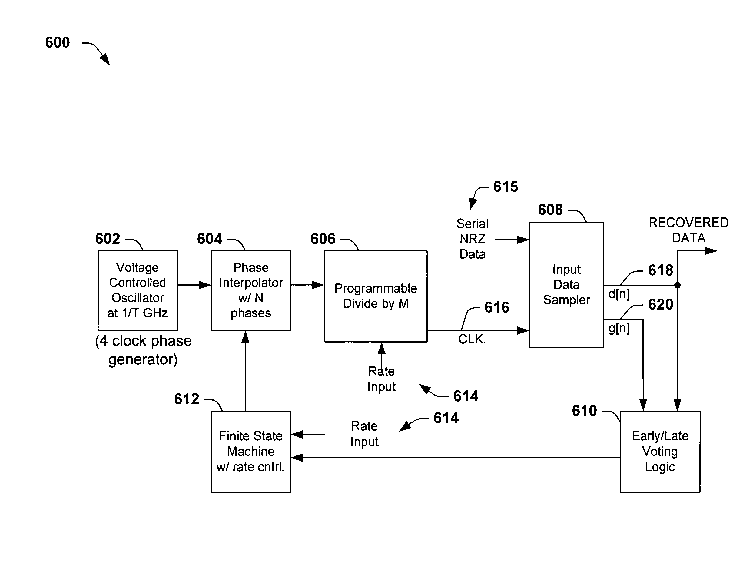
[0014]The present invention facilitates operation of clock and data recovery systems by providing systems and methods of maintaining a fixed tracking capability of an interpolator based clock and data recovery (CDR) circuit at multiple data rates. The present invention provides a wide data rate range CDR circuit using a phase interpolator optimized for a fixed frequency. In addition, the invention facilitates digitally programming the update rate and interpolator step size of the CDR circuit to provide an increased bandwidth for fast locking CDR operations, and / or a reduced bandwidth for improved tracking accuracy for use in synchronous systems. This allows the CDR circuit to be tailored to a wide variety of end-user applications.
[0018]The finite state machine (FSM) of the present invention determines which two adjacent phases of the VCO clock are selected for the DAC logic of the interpolator and the relative weightings of the two phases used in the mixer. These weightings are often the DAC codes used to drive the phase interpolator. The FSM is also logically controlled by the input data rate. The finite state machine also controls how often the phase of the output clock from the phase interpolator is updated (often called the update frequency or loop latency). The FSM of the present invention also controls the magnitude of the phase steps taken by the phase interpolator by controlling the phase selection and DAC codes such that a single update results in single or multiple steps in the output clock phase from the phase interpolator. The finite state machine may further comprise an anti-glitch circuit to prevent glitches (defined as short or missing clock pulses) at the output of the interpolator when a large number of simultaneous phase correction steps are taken. This circuitry, in one aspect of the present invention spreads out (distributes) a single large step phase correction into multiple smaller (partial) phase correction steps evenly distributed over the total time of the large phase correction step required. In this way, a large phase correction is permissible within a single interpolator update period without requiring the design of a phase interpolator capable of accurately making both large and small phase updates, which are often contrary design requirements. This prevents the interpolator from taking a large instantaneous step in its output phase, which may otherwise produce a short or missing clock pulse at the output of the phase interpolator or subsequent circuits.
[0020]The CDR of the present invention maintains a constant bandwidth at multiple data rates by allowing the phase interpolator to take multiple steps at each update for lower data rates, provided by the programming of multiple steps per update for support of the systems operating at, for example, 12.5 Gbps, 6.25 Gbps, 3.125 Gbps, 1.5625 Gbps and 1.25 Gbps. Since the phase step size is fixed with respect to the interpolator clock, as the data rate decreases, the tracking capability also decreases. For example, with a phase interpolator with 128 steps operating at 6.25 GHz (TCLK=160 ps) used in a 6.25 Gbps system, each step corresponds to 160 / 128=1.25 ps. Each step corresponds to 1 / 128th of a 6.25 Gbps unit interval (UI). When used in a 3.125 Gbps system, each step now equals only 1 / 256th of a 3.125 Gbps UI. If the update rate or step size is not adjusted, the bandwidth would be halved for the 3.125 Gbps with respect to the 6.25 Gbps system. The CDR of the present invention provides a substantially constant tracking ability over the range of data rates by keeping the number of steps referenced to the operating UI constant.
[0022]Further, the present invention provides a means to either increase the bandwidth of the CDR by increasing the number of steps per update and reducing the latency to allow for either tracking a rapidly changing input phase or to provide a fast locking CDR capability. Alternately, the invention provides a means to decrease the BW of the CDR by decreasing the number of steps per update and increasing the latency to provide for higher accuracy transition placement in slowly changing or synchronous systems.
[0023]The present invention obtains the current data rate input, sets the rate programmable divider ratio based on the obtained data rate to adjust the clock frequency to approximately match that the rate of the input data stream. It also uses the data rate input to adjust the phase correction step size. The present invention uses the adjusted size phase step to keep the BW of the CDR circuit substantially constant. Using the ELV logic, the present invention identifies an early, late, or neither indication for the recovered clock for each bit time. The present invention further distributes the phase correction step over a plurality of partial steps based on the obtained rate, which, as a result, prevents clock glitches from occurring, as would normally be associated with large phase correction steps. Thus, tracking capability is maintained regardless of the data rate or different clock recovery bandwidth is provided to suit the particular system requirements.

Problems solved by technology

If the recovered clock is too early, the clock recovery system delays the clock.
In a conventional CDR, the capture range of the PLL and / or VCO used is typically narrow, and has a disadvantage of limiting the tracking capability (or bandwidth) of the CDR circuit, particularly when a wide range of data rates is anticipated.
The analog types require many special analog components which can be difficult to implement in integrated circuit devices, and when not carefully designed may not function properly under all conditions.
This can be detrimental to the integrity of the recovered clocks if the early / late decision is actually incorrect due to jitter in the incoming data or the recovered clock.
Because of the time consumed to actually collect these samples, the large amount of processing required to identify early / late for each bit and whether the total of clocks were early or late, and the latencies of the various circuits of the system, the update rate and therefore the bandwidth of the CDR is limited.

Method used


Image

  • Interpolator based clock and data recovery (CDR) circuit with digitally programmable BW and tracking capability
  • Interpolator based clock and data recovery (CDR) circuit with digitally programmable BW and tracking capability
  • Interpolator based clock and data recovery (CDR) circuit with digitally programmable BW and tracking capability

Examples


Embodiment Construction

[0045]The present invention will now be described with respect to the accompanying drawings in which like numbered elements represent like parts. The figures provided herewith and the accompanying descriptions of the figures are merely provided for illustrative purposes. One of ordinary skill in the art should realize, based on the instant description, other implementations and methods for fabricating the devices and structures illustrated in the figures and in the following description.

[0046]The present invention facilitates clock and data recovery for serial data streams by providing a mechanism that can be employed to maintain a fixed tracking capability of an interpolator based CDR circuit at multiple data rates. The present invention further provides a wide data rate range CDR circuit, yet uses an interpolator design optimized for a fixed frequency. The invention employs a rate programmable divider circuit that operates over a wide range of clock and data rates to provide vario...


PUM


Abstract

The present invention facilitates clock and data recovery (330,716 / 718) for serial data streams (317,715) by providing a mechanism that can be employed to maintain a fixed tracking capability of an interpolator based CDR circuit (300,700) at multiple data rates (e.g., 800). The present invention further provides a wide data rate range CDR circuit (300,700), yet uses an interpolator design optimized for a fixed frequency. The invention employs a rate programmable divider circuit (606,656,706) that operates over a wide range of clock and data rates (e.g., 800) to provide various phase correction step sizes (e.g., 800) at a fixed VCO clock frequency. The divider (606,656,706) and a finite state machine (FSM) (612,662,712) of the exemplary CDR circuit (600,650,700) are manually programmed based on the data rate (614,667). Alternately, the data rate may be detected from a recovered serial data stream (718) during CDR operations (on-the-fly) utilizing a frequency detection circuit (725) to automatically program the divider (706) and FSM (712) to provide CDR circuit operation at the nearest base clock rate (716).

Description

FIELD OF THE INVENTION[0001]The present invention relates generally to high speed encoded data communications, and more particularly, to systems and methods that recover clock information from encoded serial data with digitally programmable bandwidth logic to provide fast locking capability or improved tracking accuracy.BACKGROUND OF THE INVENTION[0002]There are several common serial communication standards currently available, including USB (Universal Serial Bus) 1.1 that provides communication speeds up to 12 Mbps (Million bits per second), FireWire (IEEE 1394) that operates at 400 Mbps, and USB 2.0 that operates at a maximum of about 480 Mbps. The operational speeds of these standards have increased over time. For example, the speed of USB 2.0 versus USB 1.1 illustrates an improvement of over 40 times. State of the art optical networks used in data communications and telecommunications operates at bit rates up to 40 Gbps (billion bits per second).[0003]Generally, serial communica...

Claims


Application Information

Patent Timeline
Patent Type & Authority Patents(United States)
IPC IPC(8): H04L7/00H03L7/081H04L7/033
CPCH03L7/0814H04L7/0337H04L7/0025
Inventor PAYNE, ROBERT FLOYDPARTHASARATHY, BHARADWAJ
Owner TEXAS INSTR INC
Why Eureka
Try Eureka