Error correction for programmable logic integrated circuits

a technology of error correction and integrated circuit, which is applied in error detection/correction, instruments, computing, etc., to achieve the effect of reducing static hazards, increasing the time delay of error correcting circuitry, and reducing static hazards

Inactive Publication Date: 2008-02-05
ALTERA CORP
View PDF107 Cites 126 Cited by
  • Summary
  • Abstract
  • Description
  • Claims
  • Application Information

AI Technical Summary

Benefits of technology

[0009]In a further embodiment, error correcting circuitry can be provided that reduces static hazards resulting because of different propagation times for different paths. In one approach, a horizontal parity bit and a vertical parity bit are computed that include all the memory cells in that row and column except for the memory cell being corrected. A corrected value is computed based on the horizontal parity bit, the vertical parity bit, and the contents of the memory cell being corrected. In another approach, which uses fewer logic gates, a triple redundancy method can be implemented. Each bit of the configuration data is stored in three memory cells. Error correcting circuitry is provided that determines what same bit value is in all, or in a majority (e.g., 2 memory cells), of the three memory cells, which is then sent as output. In yet another approach, the static hazard can be minimized by slowing the logic stage of error correcting circuitry so that any possible glitch is absorbed by the logic. This can be achieved by using a logic gate with a weak drive combined with a large capacitive load. A resistive element such as a polysilicon wire, a current starved pass gate, or a current starved inverter can be used with a capacitor to increase the time delay for the error correcting circuitry.
[0010]In some instances, it may be desirable to design programmable logic IC routing architectures that reduce the number of memory cells needed to implement a given function. For example, for multiplexers that are commonly used in existing programmable logic IC architectures, error correcting circuitry can be used with encoded circuitry that results in a smaller number of memory cells needed to control the operation of the multiplexers.

Problems solved by technology

There can be one error correcting circuit associated with all the memory cells in a programmable logic IC.

Method used


Image

  • Error correction for programmable logic integrated circuits
  • Error correction for programmable logic integrated circuits
  • Error correction for programmable logic integrated circuits

Examples


Embodiment Construction

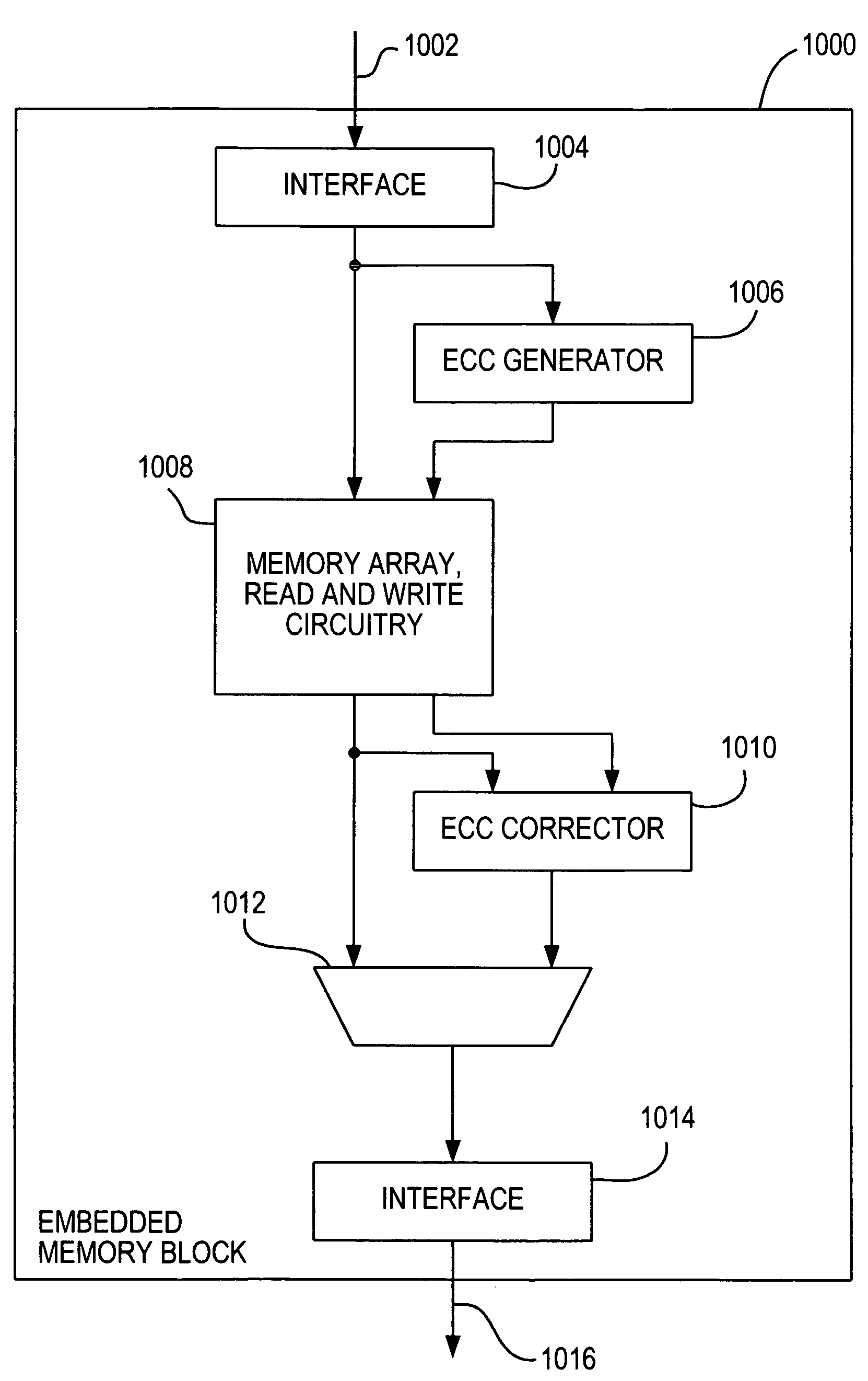
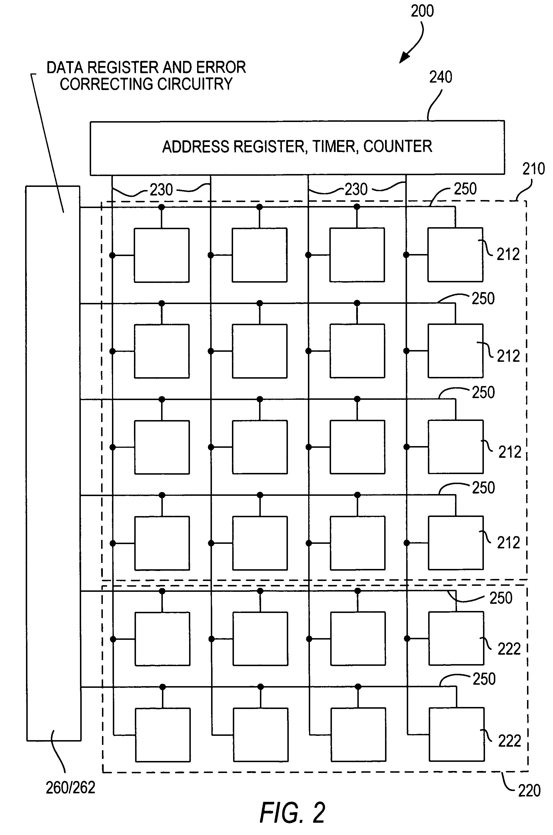
[0021]The present invention provides systems and methods for detecting and correcting errors in programmable logic ICs without the use of external logic. Programmable logic ICs include, for example, programmable logic devices, complex programmable logic devices, field-programmable gate arrays, or other suitable programmable devices. Errors include soft errors, hard errors, or both.

[0022]A programmable logic IC holds data to program that programmable logic IC to implement any of one or more various applications. This data is referred to herein as configuration data. The configuration data is represented as a set of binary digits (i.e., binary “1's” and “0's”) and may be stored in any suitable memory such as, for example, a configuration random access memory (CRAM). Alternatively, the programmable logic IC configuration data may be stored in any other suitable volatile or nonvolatile memory including, for example, static random access memory (SRAM) and dynamic random access memory (DR...


PUM


Abstract

Systems and methods for detecting and correcting errors in programmable logic ICs are provided. In one embodiment, a scrubber periodically reads the memory cells in a programmable logic IC, detects and corrects any errors, and writes the corrected contents back into the memory cell. In another embodiment, regions of memory cells in a programmable logic IC each have associated error correcting circuitry which operates to continuously detect and correct errors as they occur. Error correcting circuitry can further be designed to reduce static hazards. It may be more desirable to design programmable logic IC routing architectures that reduce the number of memory cells needed to implement a given function. Error correcting circuitry can be provided for configuration memory or for an embedded memory block on a programmable logic IC.

Description

BACKGROUND OF THE INVENTION[0001]This invention relates to programmable logic integrated circuits (ICs). More particularly, this invention relates to providing error correction for programmable logic ICs.[0002]A programmable logic IC is a general-purpose circuit that is programmable to perform any of a wide range of logic tasks. Known examples of programmable logic IC technology include programmable logic devices (PLDs), complex programmable logic devices (CPLDs), and field programmable gate arrays (FPGAs). Memory blocks may be provided on programmable logic integrated circuits and are used to store and subsequently output data or to perform various functions desired by the user.[0003]A programmable logic IC typically includes a large number of memory cells that store configuration data. When data is being programmed into the memory cells or while data is stored in the memory cells, errors can occur in the representation of the configuration data. Such errors can include hard errors...

Claims


Application Information

Patent Timeline
Patent Type & Authority Patents(United States)
IPC IPC(8): G06F11/00
CPCG06F11/106
Inventor LEWIS, DAVIDBETZ, VAUGHN
Owner ALTERA CORP
Why Eureka
Try Eureka