Heat treatment jig for semiconductor substrate

a technology of semiconductor substrate and heat treatment jig, which is applied in the direction of semiconductor/solid-state device details, packaging goods, furniture, etc., can solve the problems of deteriorating the planarity of the semiconductor substrate, increasing the leakage current of the lsi device, and difficulty in use, so as to eliminate the causes of slippage and effectively inhibit the effect of occurring

Active Publication Date: 2008-02-12
SUMITOMO MITSUBISHI SILICON CORP
View PDF17 Cites 422 Cited by
  • Summary
  • Abstract
  • Description
  • Claims
  • Application Information

AI Technical Summary

Benefits of technology

[0024]The present invention was performed in view of the above-mentioned problems and intends to provide a heat treatment jig for semiconductor substrates that in the case of a semiconductor substrate being heat treated by use of a heat treatment boat of a vertical heat treatment furnace, the stress applied on the semiconductor substrate can be diminished and thereby the slips can be suppressed from occurring, and a heat treatment method of semiconductor substrates therewith.

Problems solved by technology

In an existing heat treatment boat, in the case of the silicon substrate being supported only by a periphery portion thereof, when a semiconductor substrate having a diameter of 300 mm is heat treated, the tare stress is largely generated, resulting in difficulty to use.
The slip causes an increase in the leakage current of the LSI device and deteriorates the planarity of the semiconductor substrate.
However, in order to reduce the slips with precision by use of these heat treatment jigs that have a structure in which contact method is altered, problems are newly caused.
However, these publications do not describe of the flatness of the disc-like or ring-like supporting jig and the aggregate of the concave and salient.
As mentioned above, the reason for the slips being generated in the semiconductor substrate is due to the lack of the mechanical strength of the silicon carbide holder and furthermore the ring or disc jig that the holder supports under very high temperature heat treatment conditions.
Even when with the jig disclosed in Japanese Patent Application Laid-open No. 2003-037112, heights of the circular arc and the center protrusion on the holder are processed with precision, owing to the bending of the holder generated during the high temperature heat treatment, an error is generated between the heights of the circular arc and the center protrusion on the holder, resulting in difficulty in diminishing the slips.
However, since manufacturing cost increases, this cannot be applied to industrial mass-production.
Thus, the use of the disc-shaped or ring-shaped supporting substrate alone cannot suppress the slips that are generated in conjunction with the heat treatment from occurring.

Method used


Image

  • Heat treatment jig for semiconductor substrate
  • Heat treatment jig for semiconductor substrate
  • Heat treatment jig for semiconductor substrate

Examples


embodiments

[0067]In embodiments, with reference to FIGS. 2 through 10, configurations of ninth kinds of heat treatment jigs (10 to 90) will be explained.

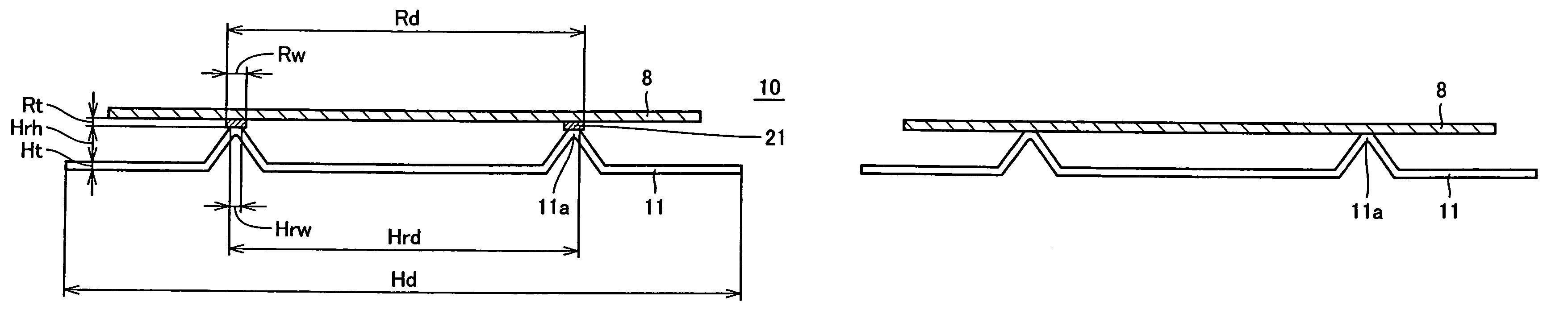
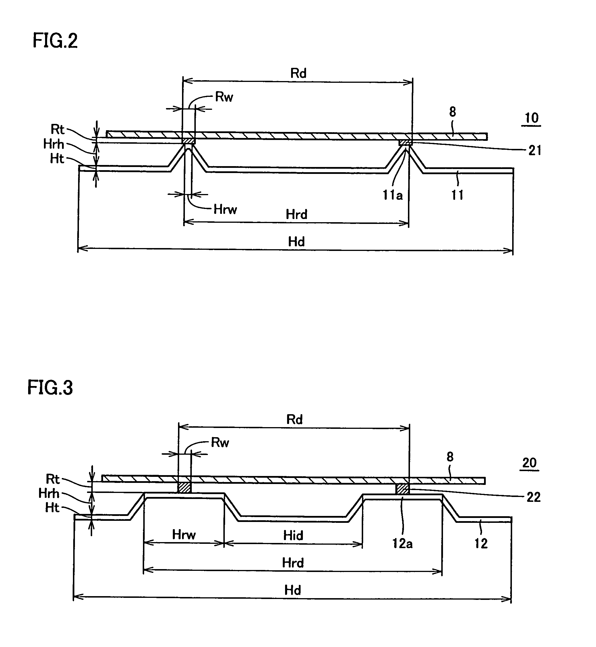
[0068]FIG. 2 is a diagram showing a configuration of a heat treatment jig 10 that is a first embodiment of the invention. A holder 11 that is used in the heat treatment jig 10 is made of vapor-phase grown silicon carbide and provided with a ring structure 11a.

[0069]The holder 11 has a diameter (Hd) of 320 mm and a thickness (Ht) of 1.3 mm; and the ring structure 11a has a diameter (Hrd) of 222 mm, a height (Hrh) of 3.5 mm and a width (Hrw) of 1.2 mm. The ring structure 11a of the holder 11 was subjected to the surface processing so that the surface roughness may be 1.6 μm and the flatness may be 185 and 20 μm.

[0070]Subsequently, on the ring structure 11a, a ring 21 made of silicon single crystal was placed. In the ring 21, an outer diameter (Rd) and a ring width (Rw), respectively, were set at 223 mm and 1.5 mm, and a thickness (Rt) was varie...


PUM

PropertyMeasurementUnit
flatnessaaaaaaaaaa
flatnessaaaaaaaaaa
surface roughnessaaaaaaaaaa

Abstract

When a two-division structure heat treatment jig for semiconductor substrate that includes a silicon first jig that comes into direct contact with a semiconductor substrate that is heat treated and supports the semiconductor substrate, and a second jig (holder) that holds the first jig and is mounted on a heat treatment boat is adopted as a heat treatment boat of a vertical heat treatment furnace, the stress concentrated during the heat treatment on a particular portion of the semiconductor substrate can be reduced; in the case of a semiconductor substrate large in the tare stress and having an outer shape of 300 mm being heat treated, or even in the case of the heat treatment being carried out under very high temperature conditions, the slips can be suppressed from occurring. The present invention can be widely applied as a stable heat treatment method of semiconductor substrates.

Description

BACKGROUND OF THE INVENTION[0001]1. Field of the Invention[0002]The present invention relates to a heat treatment jig that is used in a heat treatment boat of a vertical heat treatment furnace and a heat treatment method, and in more detail, to a heat treatment jig for a semiconductor substrate that can suppress slip generated as a crystal defect when the semiconductor substrate is heat treated at a high temperature from occurring and a heat treatment method therewith.[0003]2. Description of the Related Art[0004]A semiconductor substrate that is processed in an LSI device fabrication process, in steps of oxidation, diffusion and film deposition, is repeatedly subjected to high temperature heat treatment to fabricate. At the time of the heat treatment, when an inhomogeneous temperature distribution is caused within a plane of the semiconductor substrate, in accordance therewith the thermal stress is generated in the semiconductor substrate.[0005]On the other hand, depending on a supp...

Claims


Application Information

Patent Timeline
Patent Type & Authority Patents(United States)
IPC IPC(8): F27D5/00C30B31/00C30B31/14H01L21/48H01L23/34H01L21/673
CPCH01L21/00H01L21/67309H01L21/68Y10S414/135H01L21/324
Inventor ADACHI, NAOSHIYOSHIDA, KAZUSHIAOKI, YOSHIRO
Owner SUMITOMO MITSUBISHI SILICON CORP
Why Eureka
Try Eureka