Supercharge Your Innovation With Domain-Expert AI Agents!

Pattern design method and program of a semiconductor device including dummy patterns

a technology of semiconductor devices and dummy patterns, which is applied in the direction of semiconductor devices, instruments, computing, etc., can solve the problems of reduced yield, non-uniform size and shape, and the inability to form a dummy pattern having a pattern-covering fraction with high uniformity

Inactive Publication Date: 2008-02-19
KK TOSHIBA
View PDF10 Cites 11 Cited by
  • Summary
  • Abstract
  • Description
  • Claims
  • Application Information

AI Technical Summary

Benefits of technology

The present invention provides a method for designing a semiconductor device by creating a pattern and separating it into a dummy pattern region and a dummy pattern prohibition region. The dummy pattern region is then divided into smaller units, with inspection areas being set up to cover each unit. A tentative pattern-covering fraction is calculated for each unit, and a final pattern-covering fraction is obtained by averaging the tentative fraction. Using this final fraction, a dummy pattern is generated for each unit. The invention also provides a program for pattern design and a semiconductor device with a dummy pattern region. The technical effect of the invention is to improve the accuracy and reliability of semiconductor device design.

Problems solved by technology

When the pattern-covering fraction differs in the plane region of the semiconductor device, the following problems occur in the semiconductor manufacturing processes.
In such a case, in the manufacturing process, burying an insulating layer between wirings by use of, for example, chemical mechanical polishing process or the like, may cause a phenomenon in which a relatively large insulating layer isolation region is deeply polished, and may cause a reduction in yield.
Moreover, the pattern-covering fraction in the vicinity of the pattern differs in fine patterning processes such as lithography, relative ion etching, and the like, causing a possibility that non-uniformity in the size and the shape may occur.
However, in the conventional dummy pattern forming method, the uniform pattern-covering fraction is required over the entire dummy pattern region, causing a problem in which the pattern-covering fraction in the vicinity of the dummy pattern prohibition region is reduced to make it impossible to form a dummy pattern having a pattern-covering fraction with high uniformity.
This causes non-uniformity in the size and the shape for example.

Method used


Image

  • Pattern design method and program of a semiconductor device including dummy patterns
  • Pattern design method and program of a semiconductor device including dummy patterns
  • Pattern design method and program of a semiconductor device including dummy patterns

Examples


first embodiment

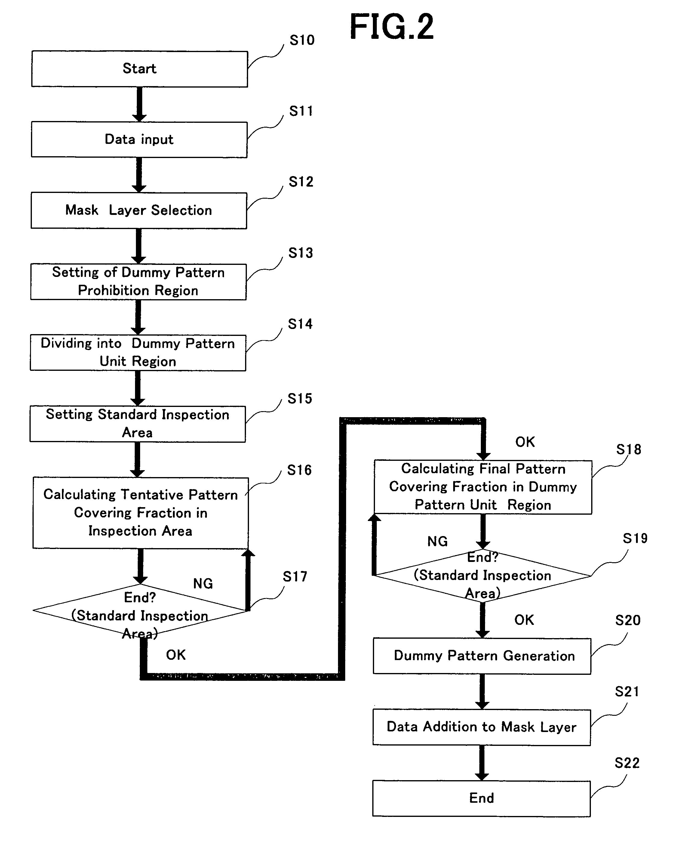
[0025]A first embodiment is an integrated circuit using MOSFETs as semiconductor devices. An explanation will be given of a method of designing a pattern with a dummy pattern taking a gate electrode layer as an example of a pattern layer.

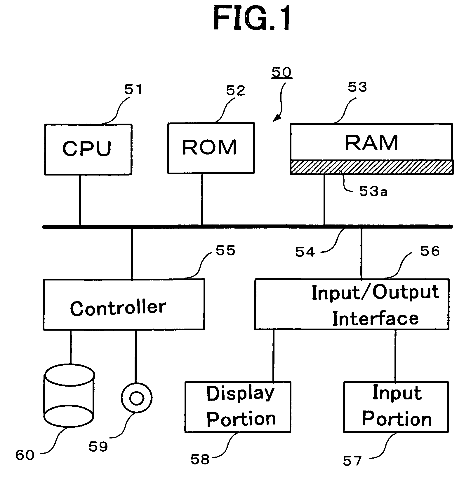
[0026]FIG. 1 is a block diagram illustrating one example of a pattern design apparatus used in executing a pattern design method for the semiconductor device according to the present invention. A pattern design program 53a, which is a computer program for carrying out pattern design of the semiconductor device, is first stored in any of storage media such as a ROM 52, a CD 59 and a disk 60 as a hard disk in a pattern design apparatus 50. The computer program stored in any of the ROM 52, the CD 52, the disk 60 or the like is passed through a bus line 54 via a controller 55 and loaded into a RAM 53. A CPU 51 executes the pattern design program 53a loaded into the RAM 53 and requests data such as a necessary parameter via an input-output interface 56 f...

second embodiment

[0044]In a second embodiment, an explanation will be given of a method of designing a mask pattern with a dummy pattern taking an example of the gate electrode layer in the integrated circuit using MOSFETs as semiconductor devices, similar to the first embodiment. In the present embodiment, an explanation will be given of a case in which the area of the inspection area is changed according to roughness and fineness of the element pattern.

[0045]The pattern design apparatus used in implementing the present embodiment is basically the same as that illustrated in FIG. 1 therefore the description is omitted.

[0046]FIG. 9 is a flowchart illustrating the steps of pattern design according to the present embodiment. In the present embodiment, after the operation is started (S40), deign data obtained when element layout design in the integrated circuit is ended is input into the storing portion such as the disk 60 of the pattern design apparatus which is basically the same as that used in the ...

third embodiment

[0063]As a third embodiment of the present invention, FIGS. 13A to 13G illustrate a method of manufacturing a semiconductor device designed as a pattern, for example, as illustrated in FIG. 8.

[0064]First of all, as illustrated in FIG. 13A, a p-type silicon substrate 30 is prepared as a semiconductor substrate, and an oxide film is selectively formed on the surface region by STI (Shallow Trench Isolation) to form an isolation region 31.

[0065]Next, phosphorus as an n-type impurity is introduced into a p-channel MISFET region in a region, which is selectively isolated by the isolation region 31 of the silicon substrate 30, using ion implantation, thereby forming an n-type well region 32. While, boron as a p-type impurity is introduced into an n-channel MISFET region using ion implantation, thereby forming a p-type well region 33. An amount of doses at this time is about 1E12 cm−2 to 1E13 cm−2 in each region. Thereafter, high-speed heating is performed, for example, at 900° C. for 10 se...


PUM


Abstract

According to an aspect of the present invention, there is provided a pattern design method of a semiconductor device, including preparing design pattern data, separating a pattern region of a semiconductor device on the basis of the design pattern data into a dummy pattern region and a dummy pattern prohibition region, dividing the dummy pattern region into dummy pattern unit regions, setting a plurality of inspection areas in the dummy pattern region and the dummy pattern prohibition region, the inspection area closing round at least the two or more dummy pattern unit regions, a part of the one dummy pattern unit region overlapping a part of another dummy pattern unit region, calculating a tentative pattern-covering fraction of a dummy pattern, the dummy pattern being formed of the dummy pattern unit region in the inspection area, calculating a final pattern-covering fraction of the dummy pattern unit region, the final pattern-covering fraction being obtained by averaging the tentative pattern-covering fraction of the dummy pattern unit region in the inspection area, and generating the dummy pattern in the dummy pattern unit region on the basis of the final pattern-covering fraction calculated on the dummy pattern unit region.

Description

CROSS REFERENCE TO RELATED APPLICATION[0001]This application is based upon and claims the benefit of priority from the prior Japanese Patent Application No. 2004-240910, filed Aug. 20, 2004, the entire contents of which are incorporated herein by reference.FIELD OF THE INVENTION[0002]The present invention relates to a semiconductor device, a pattern design method of the semiconductor device and program for the pattern design method, in particular, relates to designing a dummy pattern layout on a semiconductor device.DESCRIPTION OF THE BACKGROUND[0003]In view of the needs of the circuit design, element characteristics and the like, the patterns of elements, wirings, electrodes, and the like, which form semiconductor devices, are arranged. Accordingly, a fraction (pattern-covering fraction) indicating how much area of the plane region of the semiconductor device is occupied by these pattern areas differs depending on each semiconductor device. Moreover, these pattern areas also differ...

Claims


Application Information

Patent Timeline
Patent Type & Authority Patents(United States)
IPC IPC(8): H01L21/332
CPCH01L21/31053H01L21/32139H01L27/0207H01L2924/0002H01L2924/00
Inventor MATSUDA, SATOSHI
Owner KK TOSHIBA
Features
  • R&D
  • Intellectual Property
  • Life Sciences
  • Materials
  • Tech Scout
  • Unparalleled Data Quality
  • Higher Quality Content
  • 60% Fewer Hallucinations
Learn More