Thin, thermally enhanced molded package with leadframe having protruding region

a technology of thermal enhancement and leadframe, which is applied in the direction of semiconductor devices, semiconductor/solid-state device details, electrical apparatus, etc., can solve the problems of degrading the operational characteristics of power transistors, generating a significant amount of heat, and power semiconductor devices such as vertical mosfets (metal oxide field effect transistors)

Inactive Publication Date: 2008-02-19
SEMICON COMPONENTS IND LLC
View PDF22 Cites 48 Cited by
  • Summary
  • Abstract
  • Description
  • Claims
  • Application Information

AI Technical Summary

Benefits of technology

[0026]Embodiments of the invention have a number of advantages. First, the semiconductor die packages according to embodiments of the invention can have a low profile and two major surfaces for heat dissipation. For example, heat can be transferred away from a semiconductor die through a large source lead structure coupled to a first surface of a semiconductor die and also through a drain clip that is coupled to a second surface of the semiconductor die. The thermal resistance of this package is 35% lower than a standard SOIC (Small Outline Integrated Circuit) package and 10-15% lower than a FLMP package (Flipchip in a Leaded Molded Package). Exemplary SOIC and FLMP packages are described in U.S. Provisional Patent Application No. 60 / 349,260, filed Oct. 22, 2002. Second, embodiments of the invention can have a low profile. For example, in some embodiments of the invention, the thickness of the semiconductor die package can be from about 0.7 to about 1.0 mm. The profile of a package according to an embodiment of the invention is about 40-50% smaller than SOIC packages. This is thinner than most conventional semiconductor die packages. Because of its thin profile and its good thermal properties, a semiconductor die package according to an embodiment of the invention can be referred to as a low profile thermal enhanced flip chip in a leaded molded package (TFLMP).

Problems solved by technology

For example, power semiconductor devices such as vertical MOSFETs (metal oxide field effect transistors) can generate a significant amount of heat.
Overheating can also degrade the operational characteristics of a power transistor.

Method used


Image

  • Thin, thermally enhanced molded package with leadframe having protruding region
  • Thin, thermally enhanced molded package with leadframe having protruding region
  • Thin, thermally enhanced molded package with leadframe having protruding region

Examples


Embodiment Construction

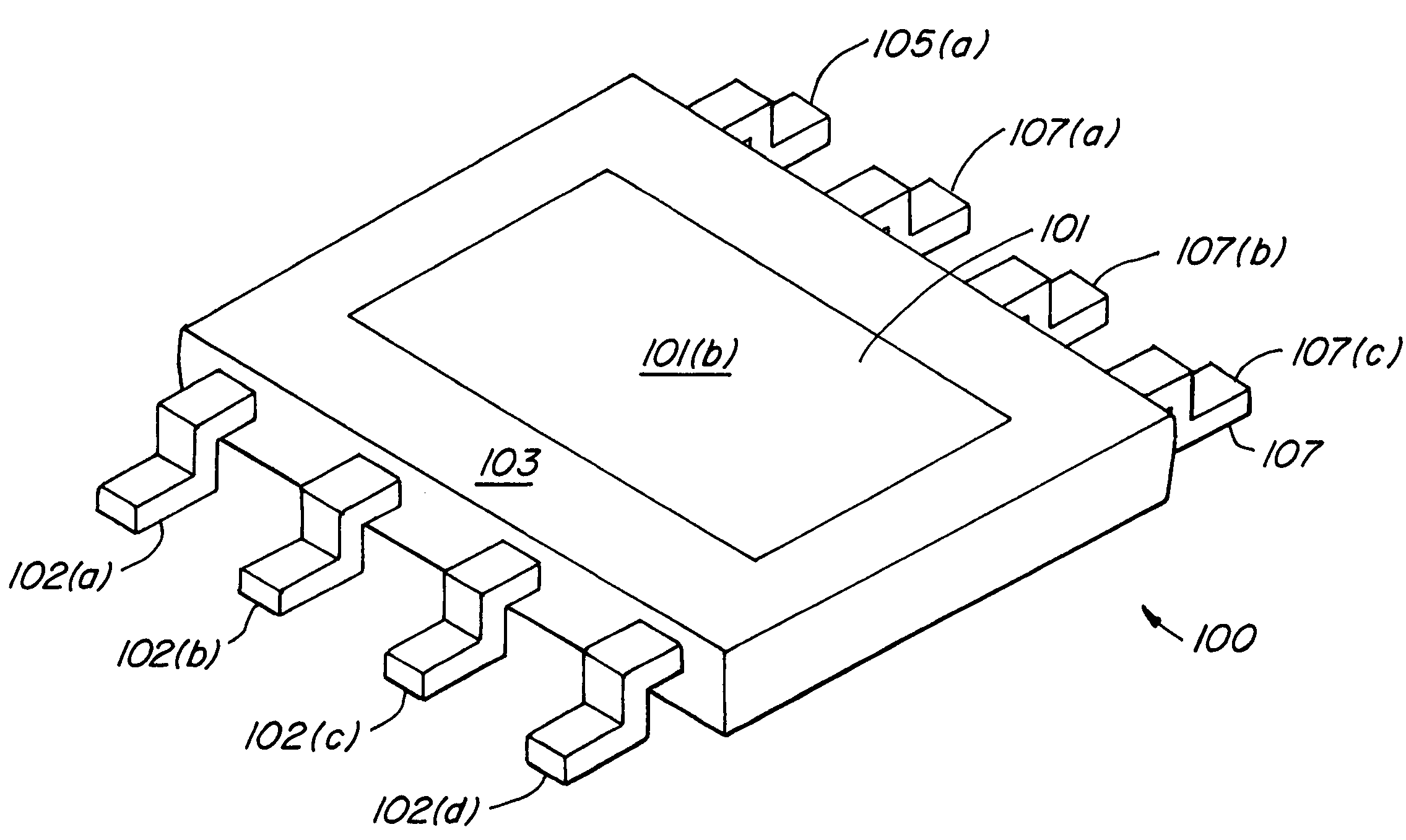
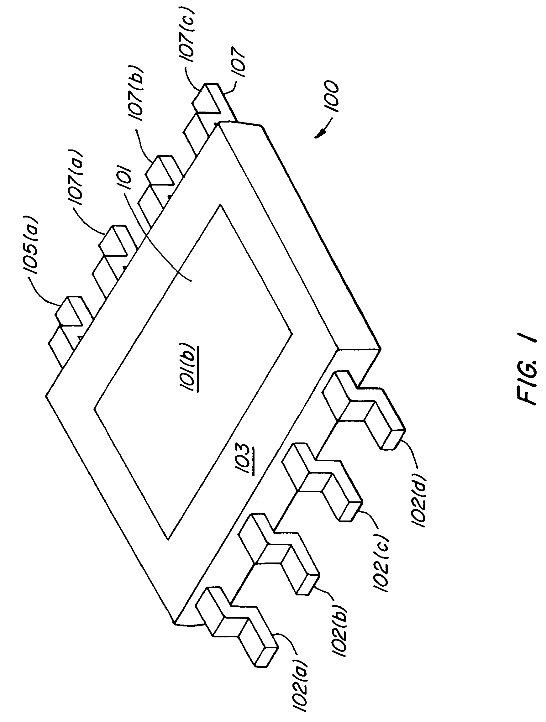
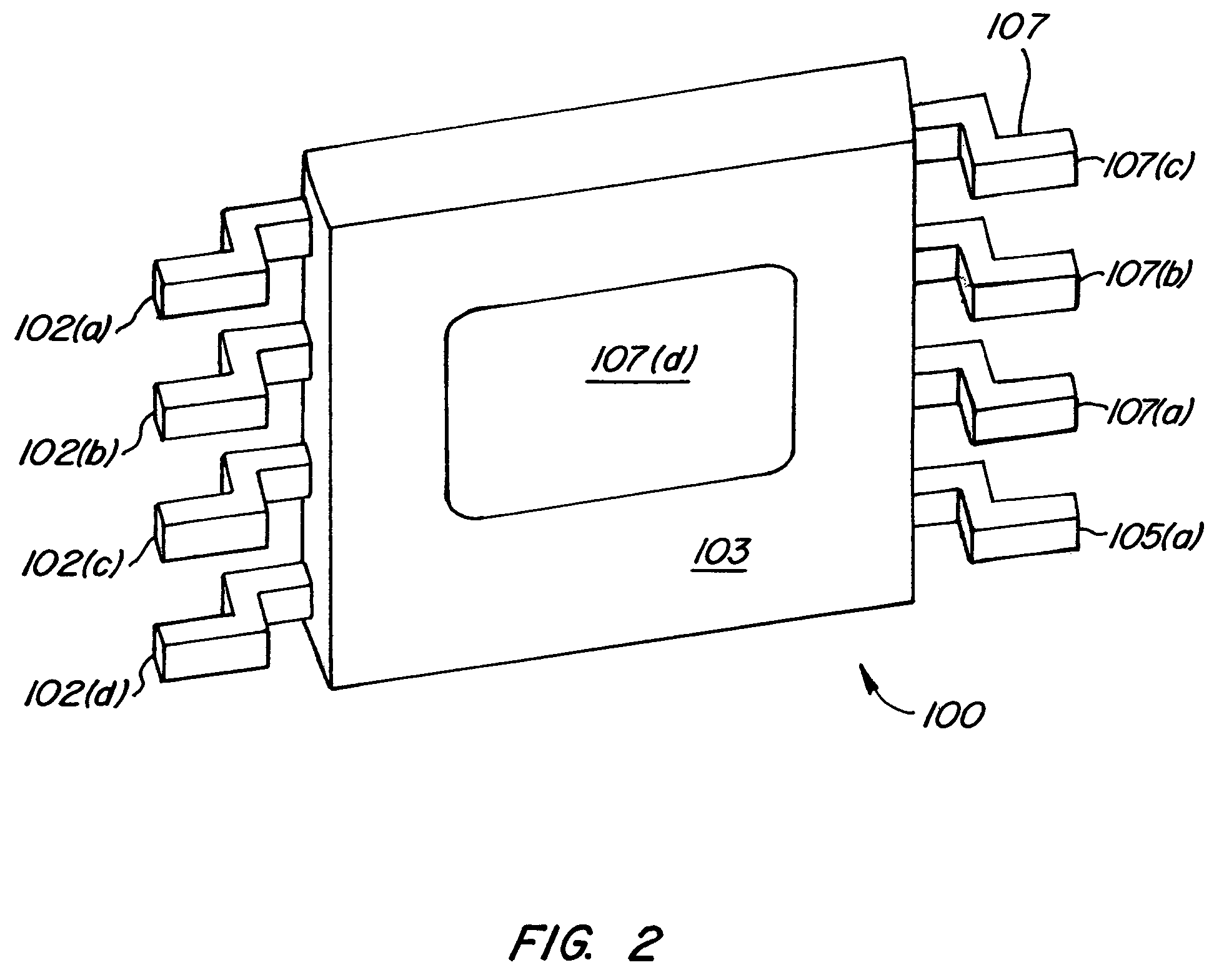
[0024]The changing architecture of power supplies, for example, on a notebook computer motherboard necessitates having a drain of a MOSFET heatsunk (as the ground) and the source and the gate (in a semiconductor die) on a different plane instead of having all three terminals on the same plane. This shift by the notebook power supply designers has led to the need to create new and improved surface mount packages.

[0025]Embodiments of the invention are directed to new and improved semiconductor die packages. In embodiments of the invention, a solder bumped semiconductor die may be flipped over and may be mounted on a lead frame structure including a source lead structure and a gate lead structure. The source lead structure may have a large down-set portion and a partially-etched (e.g., half-etched) portion. A molding material can be molded around the source lead structure, and the semiconductor die so that a surface of the semiconductor die and a surface of the partially-etched portion...


PUM


Abstract

A semiconductor die package. It includes (a) a semiconductor die including a first surface and a second surface, (b) a source lead structure including protruding region having a major surface, the source lead structure being coupled to the first surface, (c) a gate lead structure being coupled to the first surface, and (d) a molding material around the source lead structure and the semiconductor die. The molding material exposes the second surface of the semiconductor die and the major surface of the source lead structure.

Description

CROSS-REFERENCE TO RELATED APPLICATIONS[0001]This application is a continuation application of U.S. patent application Ser. No. 10 / 271,654, filed on Oct. 15, 2002, which is now U.S. Pat. No. 6,891,256, which claims the benefit of the filing date of U.S. Provisional Patent Application No. 60 / 349,260, filed Oct. 22, 2001, and U.S. Provisional Application No. 60 / 352,642, filed Jan. 29, 2002. All of the above applications are herein incorporated by reference in their entirety for all purposes.BACKGROUND OF THE INVENTION[0002]There are a number of semiconductor die packages. In one example of a semiconductor die package, a semiconductor die is mounted to a lead frame with leads. Wires couple the semiconductor die to the leads. The wires, the semiconductor die and then the most of the lead frame (except for the leads that extend outward) are then encapsulated in a molding material. The molding material is then shaped. The formed semiconductor die package includes a molded body that has le...

Claims


Application Information

Patent Timeline
Patent Type & Authority Patents(United States)
IPC IPC(8): H01L23/48H01L23/34H01L23/495H01L29/76H01L23/29H01L23/31H01L23/50
CPCH01L23/495H01L23/49548H01L23/49555H01L23/49562H01L23/49568H01L24/34H01L2924/1306H01L2224/16H01L2924/01013H01L2924/01033H01L2924/01078H01L2924/01082H01L2924/01005H01L2924/01006H01L2924/01074H01L2924/13091H01L2224/16245H01L2924/00H01L2924/181H01L2924/14H01L2224/84801H01L2924/00014H01L2224/37599H01L2224/83801H01L24/37H01L24/84H01L2224/37099
Inventor JOSHI, RAJEEVWU, CHUNG-LIN
Owner SEMICON COMPONENTS IND LLC
Why Eureka
Try Eureka