Electronic component and method for manufacturing the same

a technology of electronic applied in the field of electrical components and manufacturing methods, can solve the problems of difficult to establish the location at a high accuracy level, and achieve the effect of higher reliability level and higher reliability level

Inactive Publication Date: 2008-03-18
SKYWORKS PANASONIC FILTER SOLUTIONS JAPAN
View PDF27 Cites 4 Cited by
  • Summary
  • Abstract
  • Description
  • Claims
  • Application Information

AI Technical Summary

Benefits of technology

[0010]The outline structure of an electronic component of the present invention is that it is provided with a pattern suitable for aligning a SAW device chip or the like electronic device chip and an interconnection wire accurately to certain specified places of a package of the electronic component.

Problems solved by technology

In the above-described conventional technology, however, it is extremely difficult to establish the location at a high accuracy level, because of a displacement which occurs when silver-brazing the seam ring 110.

Method used


Image

  • Electronic component and method for manufacturing the same
  • Electronic component and method for manufacturing the same
  • Electronic component and method for manufacturing the same

Examples


embodiment 1

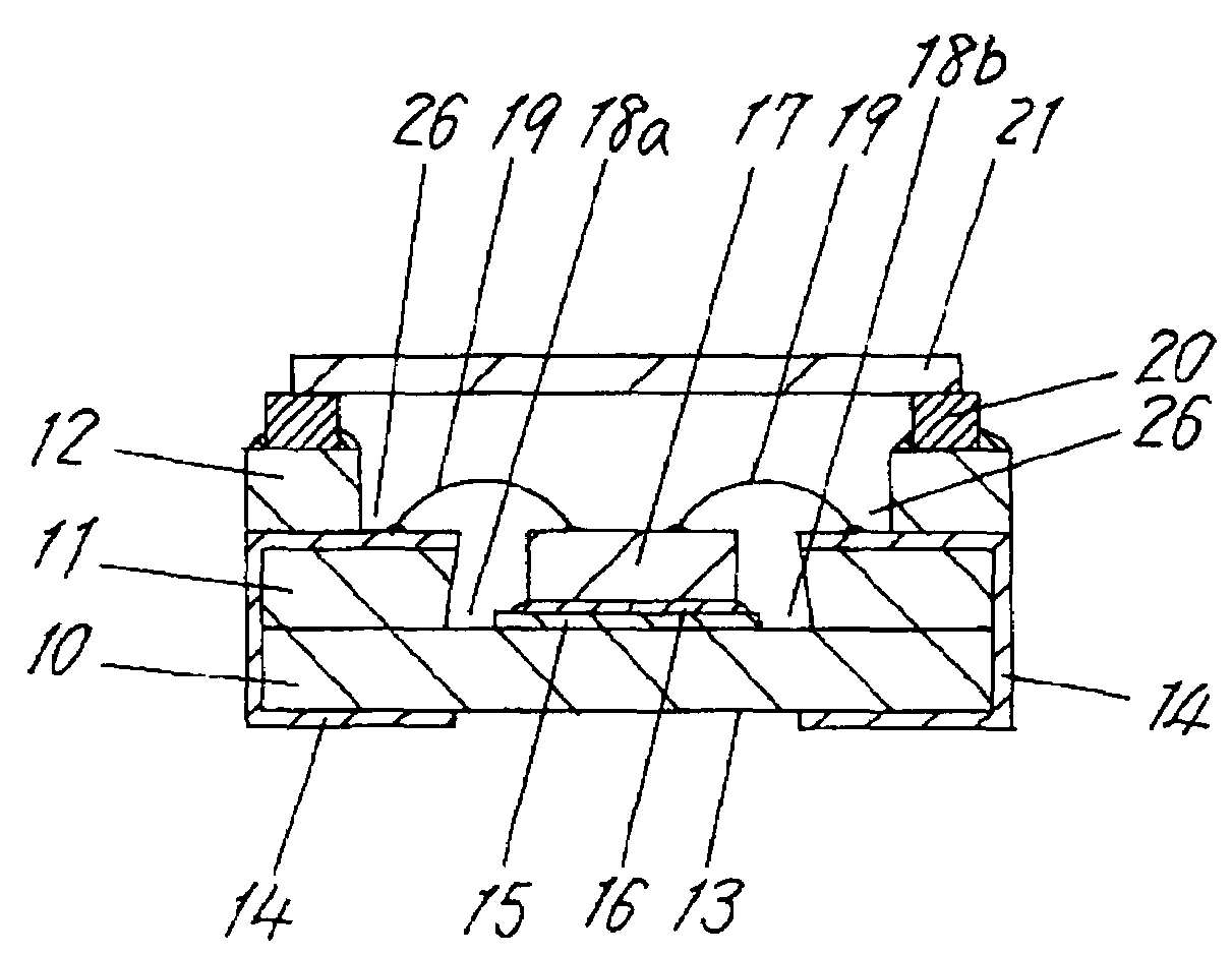
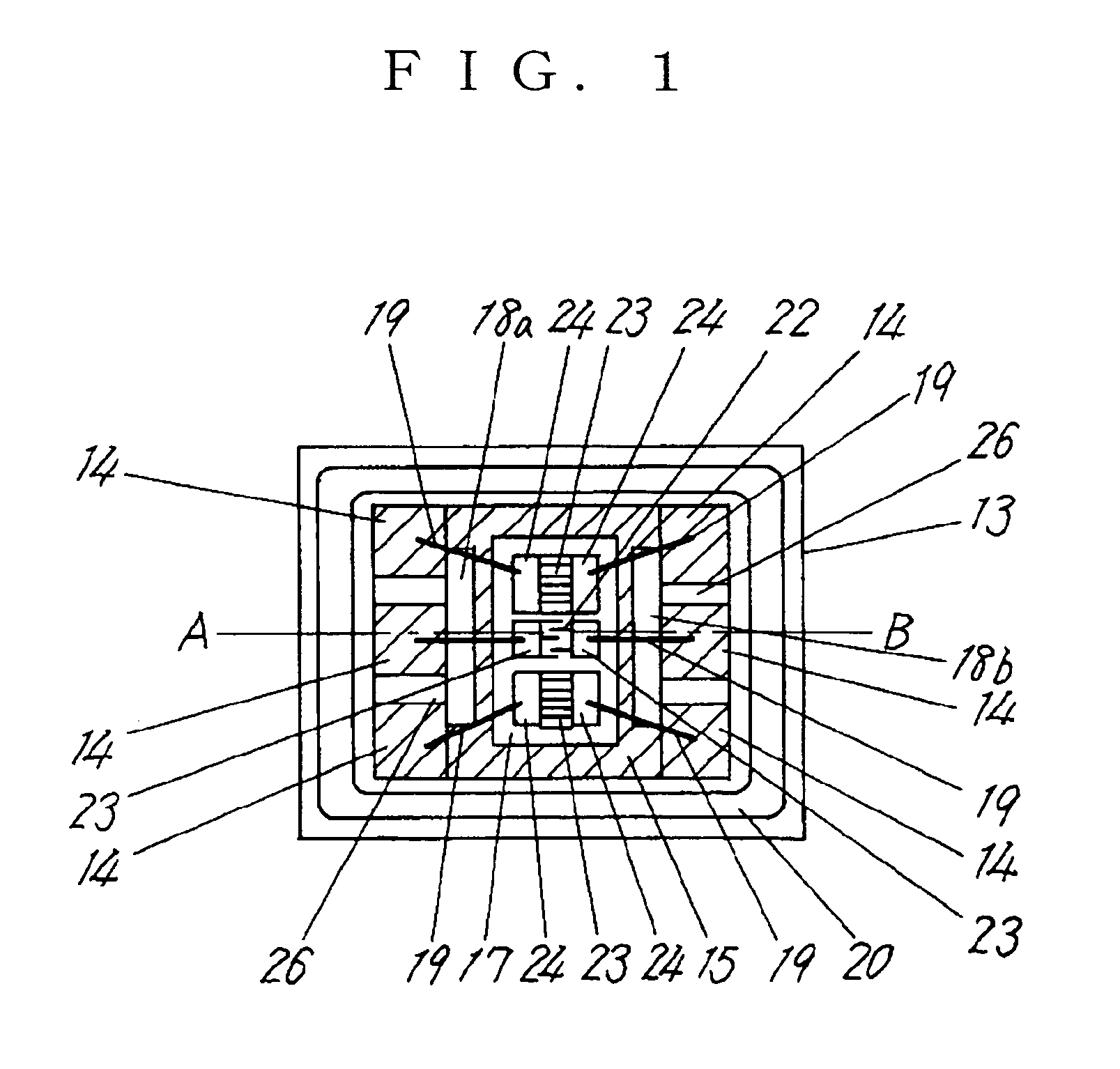
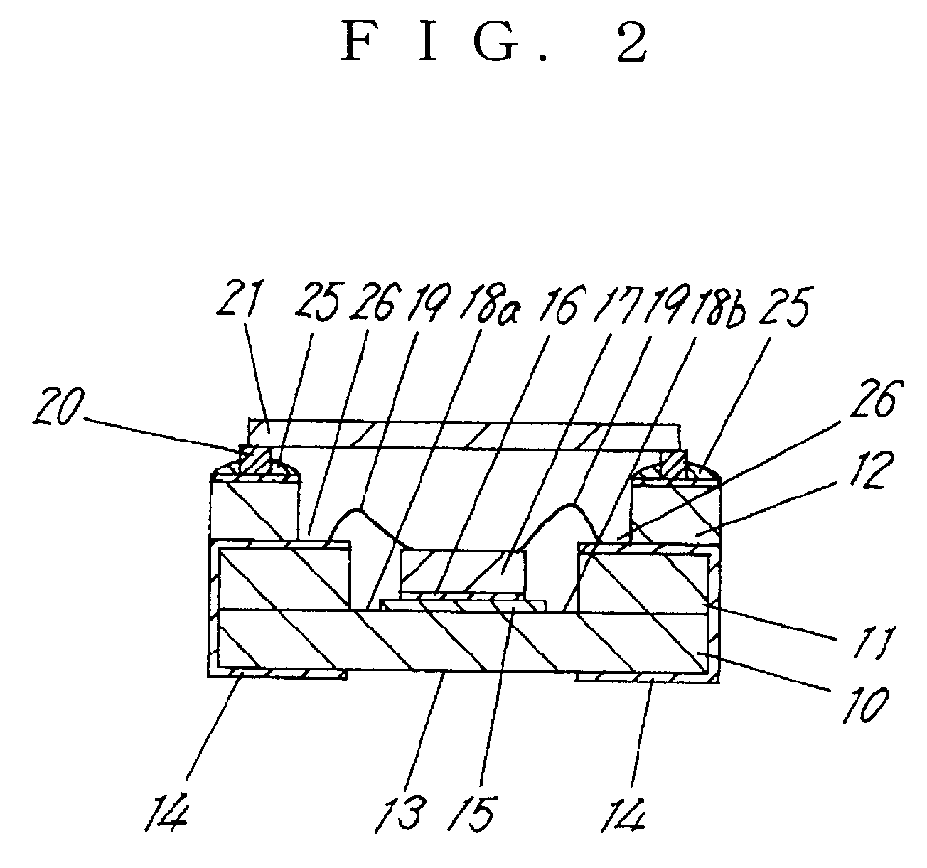
[0028]FIG. 1 shows a SAW device in accordance with a first exemplary embodiment of the present invention, as viewed from the above, or the lid side, before it is sealed with a lid. FIG. 2 shows a cross sectional view of the SAW device of FIG. 1, sectioned at the line A-B.

[0029]The first embodiment of the present invention is described in the following with reference to the drawings. On one of the surfaces of a ceramic substrate 10, namely the surface on which a SAW chip 17 is mounted, a first ceramic frame body 11 and a second ceramic frame body 12 whose size being different from the first ceramic frame body 11, are stacked in the order to form a package 13, which package having a cavity provided with a stepped level-difference 26.

[0030]An internal contact electrode 14 is formed covering one of the surfaces of the first ceramic frame body 11 (upper surface), the side faces of the ceramic substrate 10 and the first ceramic frame body 11, and part of the other surface (bottom surface)...

embodiment 2

[0043]Embodiment 2 relates to the procedure of determining a location for mounting a SAW chip 17, and the description is made with reference to FIG. 2. In the same way as in embodiment 1, a package 13 having an internal contact electrode 14 and a shield electrode 15, as well as a SAW chip 17, are prepared as the first step. The SAW chip 17 is mounted on the shield electrode 15 via an adhesion layer 16. A pattern recognition is conducted on the package 13 from the above to detect a cross point formed by the non-electrode portion 18a, 18b and the internal contact electrode 14. The middle point is established in a straight line connecting the corresponding two cross points. Using the middle point as reference, and based on various dimensional particulars of the package 13, a place for mounting a SAW chip 17 is determined.

[0044]In other words, the non-electrode portion 18a, 18b is provided for at least two, and a SAW chip 17 is placed somewhere in a straight line connecting the two. And...

embodiment 3

[0046]Embodiment 3 relates to the procedure of determining a place for bonding an interconnection wire 19 on an internal contact electrode 14. Description is made referring to FIG. 3; where, portions designated by the same numerals as in FIG. 1 represent that they perform the same functions respectively. In the following, only the points of difference from embodiment 1 are described. In embodiment 1, the is disposed immediately next to the internal contact electrodes 14, as viewed from above the package 13. However, in the present embodiment 3, the region 18a, 18b is not disposed at a place where it has an immediate contact with the internal contact electrodes 14.

[0047]Therefore, when a pattern recognizing procedure is conducted on the package 13 from the above, a cross point formed by the extension of a side of the non-electrode portion 18a, 18b, which side facing the stepped level-difference 26, and the extension of a side of the internal contact electrode 14, which side facing th...


PUM


Abstract

An electronic component, in which a chip can be mounted on a certain predetermined place of the package at a high accuracy level, which package having a stepped level-difference in the inner wall of a cavity. The package is provided with a stepped level-difference in the inner wall surface, and an internal contact electrode formed on the upper surface of the stepped level-difference. At the bottom of the package is a shield electrode, on which a chip is mounted via an adhesion layer. The chip and the internal contact electrode are electrically connected by an interconnection wire. Location aligning for the chip and the interconnection wire, at least either one of these, is conducted by making use of a region, which is non-electrode portion, provided on the inner bottom surface of the package.

Description

[0001]This application is a Continuation of application Ser. No. 09 / 856,822, filed Aug. 27, 2001, now issued as U.S. Pat. No. 6,804,103 which is a National Phase Application of PCT International Application PCT / JP00 / 06646.TECHNICAL FIELD[0002]The present invention relates to a SAW (Surface Acoustic Wave) device or the like electronic component that houses electronic device chip in the package. The present invention relates also to a method for manufacturing the electronic components.BACKGROUND ART[0003]FIG. 5 shows a plan view of a conventional SAW device, while FIG. 6 shows the cross sectional view. As shown in these drawings, a conventional SAW device is manufactured by first stacking a first ceramic frame body 101 on one of the surfaces of a ceramic substrate 100, and a second ceramic frame body 102 on the first ceramic frame body 101, and these frame bodies together with the substrate are fired to form an integrated package 103. An internal contact electrode 104 and a shield ele...

Claims


Application Information

Patent Timeline
Patent Type & Authority Patents(United States)
IPC IPC(8): H01L23/48H01L23/02H01L23/52H01L29/22H01L33/00H01L23/552H01L23/12H01L21/50H01L21/60H01L23/057H01L23/13H03H9/25
CPCH01L21/50H01L23/057H03H9/1071H01L23/13H01L23/552H01L24/80H01L2224/73265H01L2224/48227H01L2224/32225H01L2924/014H01L2924/01074H01L2924/01047H01L2924/01005H01L24/49H01L24/48H01L2224/48091H01L2224/49171H01L2224/49175H01L2224/83136H01L2924/01013H01L2924/01033H01L2924/01078H01L2924/01079H01L2924/01082H01L2924/15153H01L2924/1517H01L2924/1617H01L2924/16195H01L2924/3025H01L2924/00014H01L2924/00H01L2924/15787H01L2224/05599H01L2224/8547H01L2224/45099H01L2224/45015H01L2924/207H01L21/60
Inventor MURAKAMI, KOZOFUJII, KUNIHIROMATSUO, SATOSHI
Owner SKYWORKS PANASONIC FILTER SOLUTIONS JAPAN
Why Eureka
Try Eureka