Chip antenna

a chip antenna and antenna technology, applied in the direction of resonant antennas, helical antennas, non-resonant long antennas, etc., can solve the problems of increasing the difficulty of miniaturizing chips, requiring even lower resonance frequency in the same volume, and limiting the ability to maintain a miniaturized structur

Inactive Publication Date: 2008-04-08
SAMSUNG ELECTRO MECHANICS CO LTD
View PDF4 Cites 83 Cited by
  • Summary
  • Abstract
  • Description
  • Claims
  • Application Information

AI Technical Summary

Benefits of technology

[0012]It is another object of the invention to provide a chip antenna capable of achieving broadband of the desired resonance frequency without being increased in size.

Problems solved by technology

A chip antenna installed in a Bluetooth or a Wireless Local Area Network (WLAN) mobile telecommunication terminal requires relatively low frequency band, and thus has longer conductor patterns constituting a radiation element to obtain a sufficient length of electric resonance, which makes the chip antenna more difficult to be miniaturized.
However, mobile telecommunication terminals are further miniaturized recently and thus a chip antenna with even lower resonance frequency in a same volume is required.
In the meantime, it is desirable for the chip antenna to achieve resonance frequency band as wide as possible to maintain sending and receiving capabilities in the changing external conditions, but there is a limitation as to maintaining a miniaturized structure and achieving wide resonance frequency band as desired at the same time.

Method used


Image

  • Chip antenna
  • Chip antenna
  • Chip antenna

Examples


Embodiment Construction

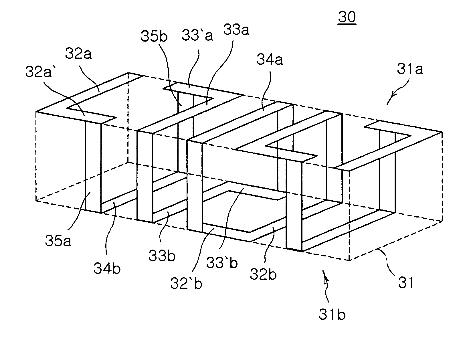
[0031]Preferred embodiments of the present invention will now be described in detail with reference to the accompanying drawings.

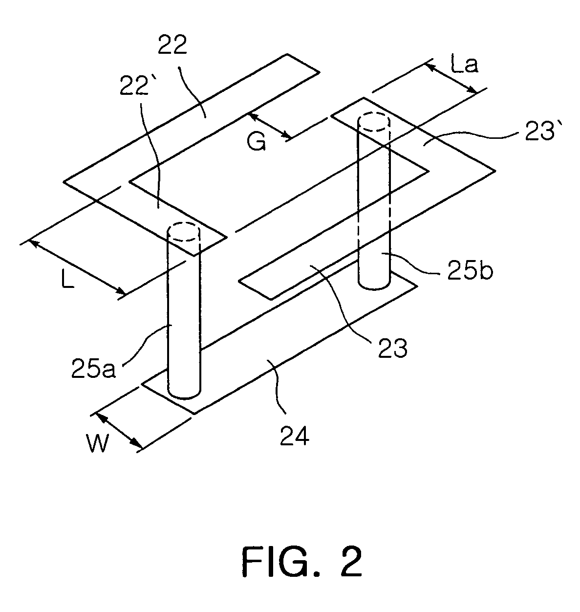
[0032]FIG. 2 is a perspective view illustrating conductor pattern structure adoptable in an embodiment of the present invention. The conductor pattern structure in FIG. 2 is an example for explaining the integration method of the present invention, and such a structure allows increased resonance length than in a dielectric block of the same volume.

[0033]With reference to FIG. 2, a pair of L-shaped conductor pattern 22 and symmetrical L-shaped conductor pattern 23 is disposed on an upper part of the dielectric block and a vertical-connecting conductive pattern 24 is disposed on a lower part of the dielectric block. The L-shaped conductor pattern 22 and the symmetrical L-shaped conductor pattern 23 are bent to face each other, having bent parts 22′ and 23′ extended in a predetermined length L. The bent parts 22′ and 23′ are disposed to overlap each other in ...


PUM


Abstract

The present invention relates to a chip antenna including first and second conductor patterns formed on upper and lower surfaces of a dielectric block in a width direction of the dielectric block. The chip antenna also includes conductive vertical-connecting parts formed in a vertical direction of the dielectric block to connect the first conductor patterns with the second conductor patterns to form a radiation line. The first and second conductor patterns comprise pairs of L-shaped and symmetrical L-shaped conductor patterns having bent parts overlapped in part with each other in a width direction and extended in a longitudinal direction of the dielectric block. Also, horizontal-connecting conductor patterns are formed in a width direction of the dielectric block.

Description

CLAIM OF PRIORITY[0001]This application claims the benefit of Korean Patent Application No. 2005-0000267 filed on Jan. 3, 2005, in the Korean Intellectual Property Office, the disclosure of which is incorporated herein by reference.BACKGROUND OF THE INVENTION[0002]1. Field of the Invention[0003]The present invention relates to a chip antenna, and more particularly, to a chip antenna having a new mono-pole structure which enables achievement of low and broadband resonance frequency without increasing volume.[0004]2. Description of the Related Art[0005]In general, miniaturization in mobile telecommunication terminals has brought necessity of miniaturization of chip antennas as well. The miniaturized chip antenna is manufactured by using a single dielectric block or depositing plural dielectric sheets to form a dielectric block and then forming conductor patterns constituting radiation element on the dielectric block.[0006]A chip antenna installed in a Bluetooth or a Wireless Local Are...

Claims


Application Information

Patent Timeline
Patent Type & Authority Patents(United States)
IPC IPC(8): H01Q1/36H01Q1/24H01Q1/38H01Q5/00H01Q9/04H01Q5/371
CPCH01Q1/22H01Q1/2283H01Q5/371H01Q11/08H01Q1/362H01Q23/00
Inventor LEE, JAE CHAN
Owner SAMSUNG ELECTRO MECHANICS CO LTD
Why Eureka
Try Eureka