

High speed laser scanning inspection system
a laser scanning and inspection system technology, applied in the field of systems and methods for detecting irregularities on a substrate, can solve the problems of reducing optical power, undesirable coherent phenomena in imaging systems, and adding to system complexity, so as to achieve rapid inspection of a substrate
- Summary
- Abstract
- Description
- Claims
- Application Information
AI Technical Summary
Benefits of technology
Problems solved by technology
Method used
Image

Examples
first embodiment
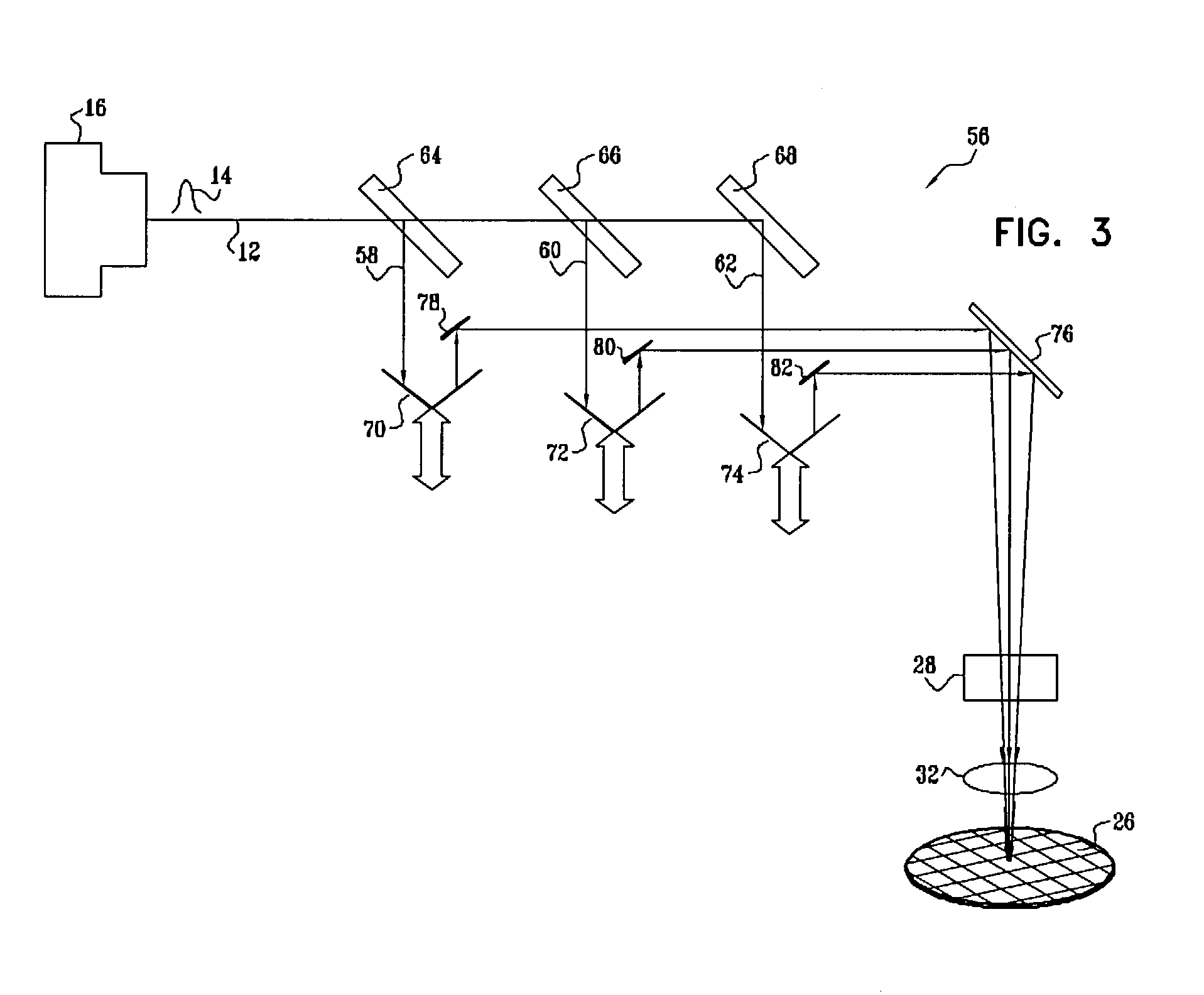
[0081]Reference is now made to FIG. 3, which is a schematic illustration of an optical inspection system 56, which is constructed and operative in accordance with a disclosed embodiment of the invention.
[0082]The beam 12 is split into a plurality of beamlets 58, 60, 62 by beamsplitters 64, 66, 68, respectively. The relative reflectance and transmittance of each of the beam-splitters 64, 66, 68 are typically (but not necessarily) chosen so that all the beamlets 58, 60, 62 have equal intensities. The beamlets 58, 60, 62 are received respectively by retro-reflectors 70, 72, 74. The beamlets 58, 60, 62 are then directed to a reflector 76 by reflectors 78, 80, 82, after which they pass through the scanner 28, beam processing optics 34 and focusing optics 32, and impinge on the substrate 26. The retroreflectors 70, 72, 74 form free-space delay lines. They are disposed so that the optical paths of the beamlets 58, 60, 62 are of different lengths. Thus, the beamsplitters 64, 66, 68 and the ...
second embodiment
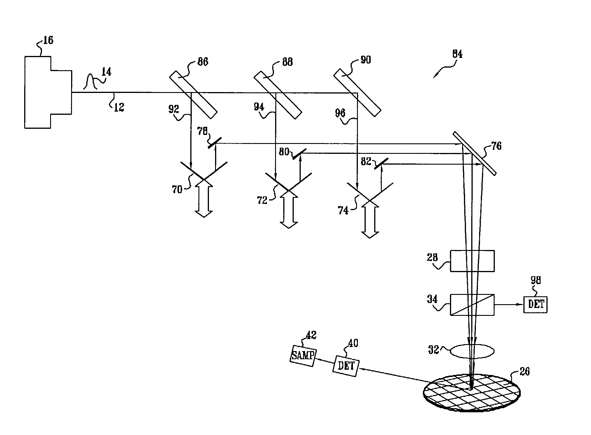
[0085]Reference is now made to FIG. 4, which is a schematic illustration of an optical inspection system 84, which is constructed and operative in accordance with an alternate embodiment of the invention. The description of FIG. 4 should be read in conjunction with FIG. 3. The arrangement of the system 84 is similar to the system 56, except now, the beamsplitters 64, 66, 68 (FIG. 3) are replaced by a series of reflective edge filters 86, 88, 90, which produce beamlets 92, 94, 96, each having a unique waveband.
[0086]The ultrafast pulse 14 inherently contains a large spectral bandwidth, with a minimum bandwidth Δv given by: Δv·τ≅1. The beamlets 92, 94, 96 are spatially separated, and not only are dispersed temporally as disclosed in the discussion of the embodiment of FIG. 3, but are also distributed according to wavelength, using the edge filters 86, 88, 90, which disperse the beamlets 92, 94, 96 according to wavelength. For example, a typical 100 fsec pulse with a central wavelength...
third embodiment
[0089]Reference is now made to FIG. 5, which is a schematic illustration of an optical inspection system 100, which is constructed and operative in accordance with an alternate embodiment of the invention. The system 100 is similar to the system 84 (FIG. 4). However, different time delays for the beamlets 92, 94, 96 are now achieved by transmitting the beamlets 92, 94, 96 respectively through optical fibers 102, 104, 106, each fiber having a different length. Thus, the optical paths followed by the beamlets 92, 94, 96 have unique lengths.
PUM
| Property | Measurement | Unit |
|---|---|---|
| operational spectral width | aaaaa | aaaaa |
| operational spectral width | aaaaa | aaaaa |
| diameters | aaaaa | aaaaa |
Abstract
Description
Claims
Application Information