Automatic supervised classifier setup tool for semiconductor defects

a technology of automatic supervised classification and defect detection, applied in the field of semiconductor device inspection, can solve the problems that users may also be presented with defects from each class, and achieve the effects of low confidence level, efficient setting up and maintaining, and optimization of manual classification efficiency

Active Publication Date: 2008-04-15
KLA TENCOR TECH CORP
View PDF13 Cites 40 Cited by
  • Summary
  • Abstract
  • Description
  • Claims
  • Application Information

AI Technical Summary

Benefits of technology

[0008]Accordingly, mechanisms are provided for efficiently setting up and maintaining a defect classification system. In general terms, the setup procedure optionally includes automatically grouping a set of provided defects (e.g., defect images) and presenting a representative set from each defect group to the user for classification. Alternatively, a representative set from the whole defect set may be presented to the user for classification without first grouping the defects into groups. The representative set does not include all of the defects and is selected to optimize manual classification efficiency. After the initial manual classification

Problems solved by technology

After the automatic classification operation, the user may also be pres

Method used


Image

  • Automatic supervised classifier setup tool for semiconductor defects
  • Automatic supervised classifier setup tool for semiconductor defects
  • Automatic supervised classifier setup tool for semiconductor defects

Examples


Embodiment Construction

[0030]Reference will now be made in detail to a specific embodiment of the invention. An example of this embodiment is illustrated in the accompanying drawings. While the invention will be described in conjunction with this specific embodiment, it will be understood that it is not intended to limit the invention to one embodiment. On the contrary, it is intended to cover alternatives, modifications, and equivalents as may be included within the spirit and scope of the invention as defined by the appended claims. In the following description, numerous specific details are set forth in order to provide a thorough understanding of the present invention. The present invention may be practiced without some or all of these specific details. In other instances, well known process operations have not been described in detail in order not to unnecessarily obscure the present invention.

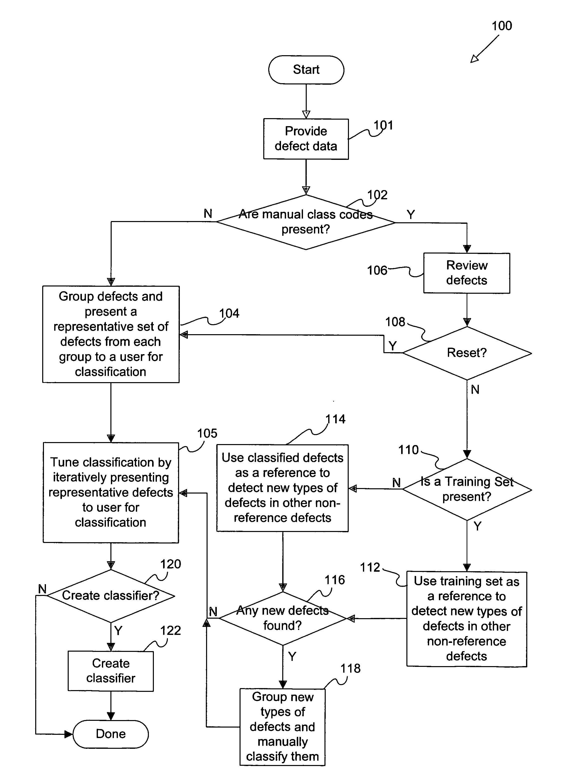
[0031]FIG. 1 is a flowchart illustrating a procedure 100 for increasing the efficiency of manual classificat...


PUM


Abstract

Disclosed are methods and apparatus for efficiently setting up and maintaining a defect classification system. In general terms, the setup procedure optionally includes automatically grouping a set of provided defects and presenting a representative set from each defect group to the user for classification. After the initial manual classification of the representative defects, the setup procedure includes an automatic procedure for classifying the non-reviewed or unclassified defects based on the manual class codes from the user-reviewed defects. After the automatic classification operation, the user may also be presented with defects from each class which may require re-classification. In particular embodiments, the user is iteratively presented with defects which have classifications that are suspect, which are near classification boundaries, or have classifications that have a low confidence level until each class is pure or contains a same type of defect classes as assigned by the user.

Description

CROSS REFERENCE TO RELATED APPLICATIONS[0001]This application claims priority of U.S. Provisional Application No. 60 / 447,360, filed on 12 Feb. 2003, which application is herein incorporated by reference in its entirety for all purposes.BACKGROUND OF THE INVENTION[0002]The present invention relates generally to inspection of semiconductor devices, such as test structures and other types of semiconductor structures. More specifically, it relates to techniques for classifying defects found on integrated circuit devices.[0003]Semiconductor defects may include structural flaws, residual process material and other surface contamination which occur during the production of semiconductor wafers. Defects are typically detected by a class of instruments called inspection tools. Such instruments automatically scan wafer surfaces and detect, and record the location of anomalies using a variety of techniques. This information, or “defect map,” is stored in a computer file and sent to a defect re...

Claims


Application Information

Patent Timeline
IPC IPC(8): G06K9/00G06K9/62G06T7/00
CPCG06K9/6253G06T7/0004G06F18/40
Inventor GAO, LISHENGMAGLUYAN, BOZHANG, JIANXINYEUNG, KEVINWU, KENONGHUANG, TONG
Owner KLA TENCOR TECH CORP
Why Eureka
Try Eureka