Apparatus for correcting solid-state electronic image sensing device
- Summary
- Abstract
- Description
- Claims
- Application Information
AI Technical Summary
Benefits of technology
Problems solved by technology
Method used
Image


Examples
Embodiment Construction
[0020]Preferred embodiments of the present invention will now be described in detail with reference to the drawings.
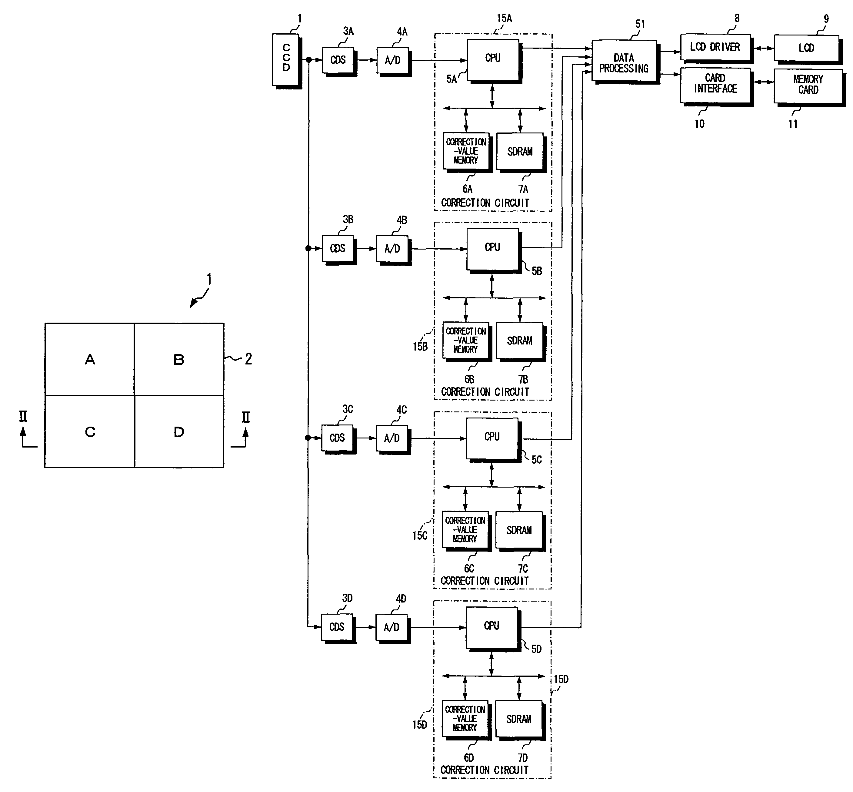
[0021]When a CCD is created, a photomask is placed on a silicon wafer and the wafer is exposed through the photomask. It is difficult to create a large-capacity CCD (e.g., one having 20 to 30 M pixels or more) at one time. Usually, exposure is performed in each of a number of different areas of the CCD, namely multiple times per CCD.
[0022]FIG. 1 is a diagram illustrating the image sensing area of a large-capacity CCD.
[0023]As shown in FIG. 1, a large-capacity CCD 1 has an image sensing area 2 in which a plurality of areas A to D have been defined. The large-capacity CCD 1 is created by performing exposure in each of the plurality of areas A to D.
[0024]By forming the image of a subject on the image sensing area 2 of the large-capacity CCD 1 using an imaging lens or the like, a video signal representing the image of the subject is output by the CCD 1.
[0025]FIG. 2 is a gr...
PUM
 Abstract
Description
Claims
Application Information