Semiconductor package and substrate having multi-level vias fabrication method

a technology of semiconductors and substrates, applied in the field of substrates, can solve the problems of insufficient plating of vias, inability to meet the requirements of increasing the density of terminal arrays, and the limitation of the number of terminals, so as to reduce the diameter of the via in the semiconductor, maintain the plating aspect ratio, and reduce the formation time of the via

Inactive Publication Date: 2008-04-29
AMKOR TECH SINGAPORE HLDG PTE LTD
View PDF155 Cites 25 Cited by
  • Summary
  • Abstract
  • Description
  • Claims
  • Application Information

AI Technical Summary

Problems solved by technology

As semiconductor die circuit complexity has increased, the number of electrical connections has generally increased, causing a need for increasingly dense terminal arrays.
However, the minimum via diameter still provides a limitation on either the number of terminals (due to deletion of terminals in via areas) or the terminal spacing (due to the presence of vias between terminals).
In particular, a via will not plate properly when the circuit pattern is large compared to the via.

Method used


Image

  • Semiconductor package and substrate having multi-level vias fabrication method
  • Semiconductor package and substrate having multi-level vias fabrication method
  • Semiconductor package and substrate having multi-level vias fabrication method

Examples


Embodiment Construction

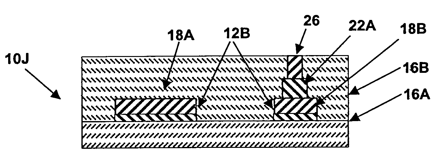
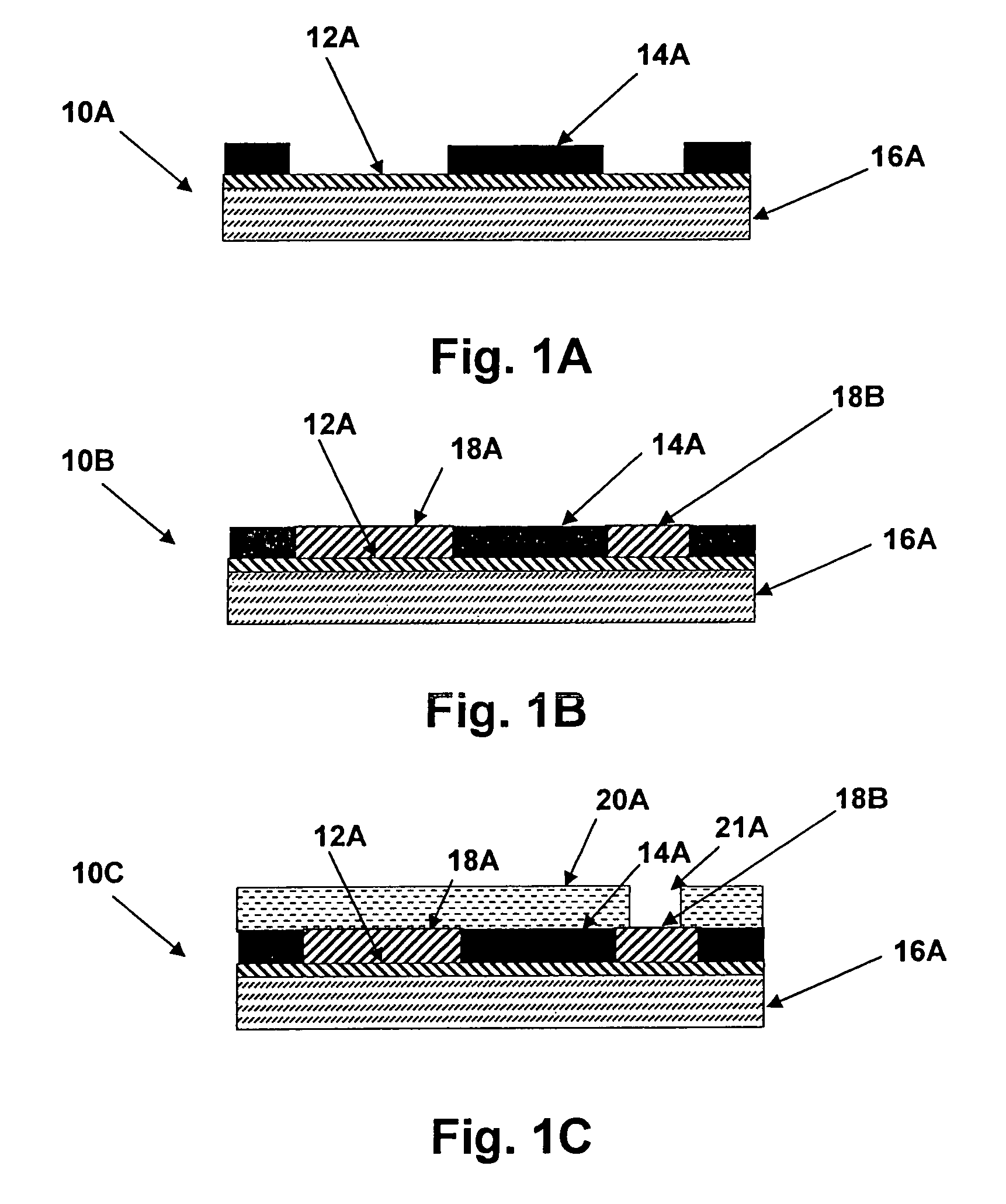
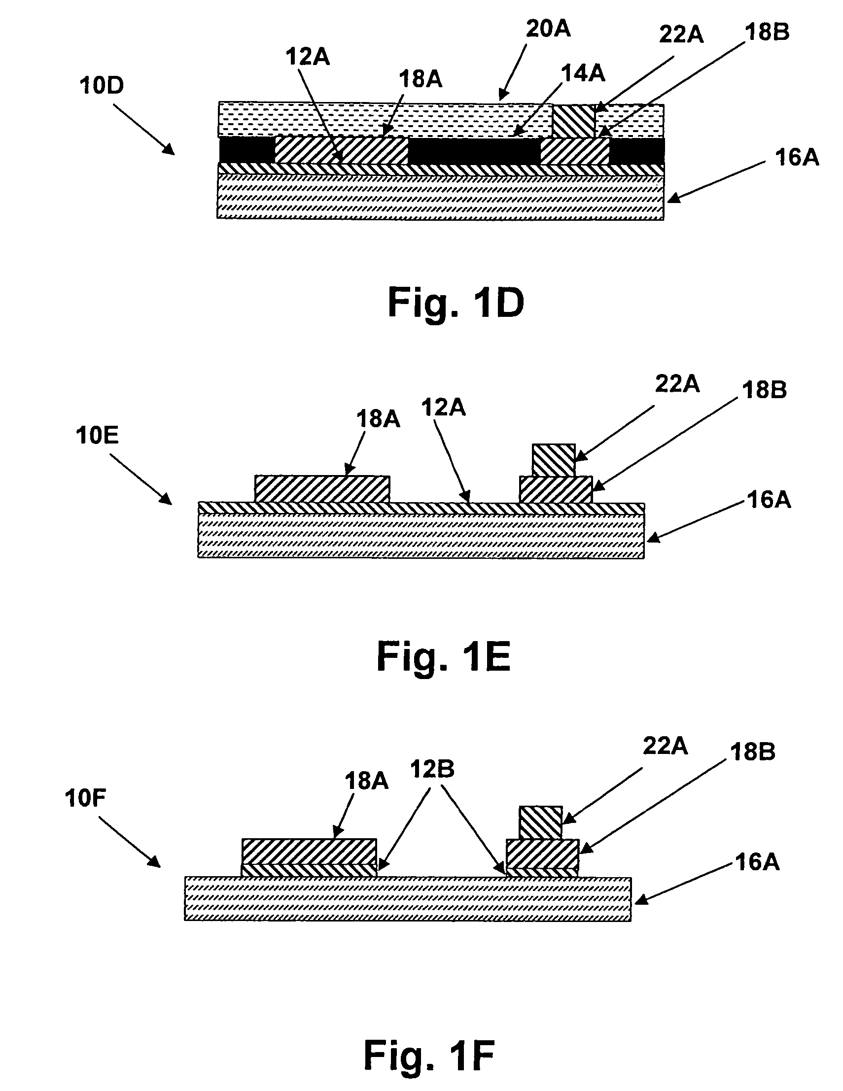
[0017]Referring now to the figures and in particular to FIGS. 1A-1H, a cross-sectional view of stages of preparation of a substrate in accordance with an embodiment of the present invention is shown.

[0018]FIG. 1A shows a first stage 10A in preparation of a substrate. A metal covered dielectric 16A may be formed by depositing or laminating a metal, generally copper, and planarizing / reducing the metal to yield a very thin metal layer 12A that will be plated over and then un-plated areas will be etched away in subsequent process steps. A resist mask 14A is applied over metal layer 12A, generally by a dry-film photo-masking process. The mask is a negative image of circuit patterns to be generated on substrate 10A in a plate-up process.

[0019]FIG. 1B shows a next state of preparation of substrate stage 10B. Metal, also generally copper, is plated over the exposed regions between plating resist 14A patterns to form circuit patterns 18A and 18B. Next, as shown in FIG. 1C, a second resist ma...


PUM


Abstract

A semiconductor package and substrate having multi-level plated vias provide a high density blind via solution at low incremental cost. Via are half-plated atop a circuit pattern and then a second via half is added to complete the via after isolation of elements of the circuit pattern. Successive resist pattern applications and etching are used to form a via tier atop a circuit pattern that is connected by a thin plane of metal. After the tier is deposited, the thin metal plane is etched to isolate the circuit pattern elements. Dielectric is then deposited and the top half of the via is deposited over the tier. The tier may have a larger or smaller diameter with respect to the other half of the via, so that the via halves may be properly registered. Tin plating may also be used to control the etching process to provide etching control.

Description

CROSS REFERENCE TO RELATED APPLICATION[0001]This application is a divisional of Huemoeller, U.S. patent application Ser. No. 10 / 839,647, filed on May 5, 2004, entitled “SEMICONDUCTOR PACKAGE AND SUBSTRATE HAVING MULTI-LEVEL VIAS”, which is herein incorporated by reference in its entirety.FIELD OF THE INVENTION[0002]The present invention relates generally to semiconductor packaging, and more specifically, to a substrate having vias generated formed in sections.BACKGROUND OF THE INVENTION[0003]Semiconductors and other electronic and opto-electronic assemblies are fabricated in groups on a wafer. Known as “dies”, the individual devices are cut from the wafer and are then bonded to a carrier. The dies must be mechanically mounted and electrically connected to a circuit.[0004]Semiconductor dies are typically packaged in a semiconductor package that includes terminals for electrically and often mechanically connecting the semiconductor package to an external device, such as a printed circ...

Claims


Application Information

Patent Timeline
Patent Type & Authority Patents(United States)
IPC IPC(8): H01L21/4763
CPCH01L21/486H01L23/49822H01L23/49827H01L2224/16H01L2224/16235H01L2924/01078H01L2924/15311H01L24/48H01L2224/48235H01L2924/00014H01L2924/15173H01L2924/00011H01L2224/0401H01L2224/45099H01L2224/45015H01L2924/207
Inventor HUEMOELLER, RONALD PATRICKHINER, DAVID JONRUSLI, SUKIANTO
Owner AMKOR TECH SINGAPORE HLDG PTE LTD
Why Eureka
Try Eureka