

Process for fabricating an integrated circuit package with reduced mold warping
a technology of integrated circuits and molds, applied in the direction of electrical equipment, semiconductor devices, semiconductor/solid-state device details, etc., can solve the problems of limiting the packaging density of such prior art devices, package disadvantages, and gang strip warping, etc., to inhibit package warping
- Summary
- Abstract
- Description
- Claims
- Application Information
AI Technical Summary
Benefits of technology
Problems solved by technology
Method used
Image

Examples
Embodiment Construction
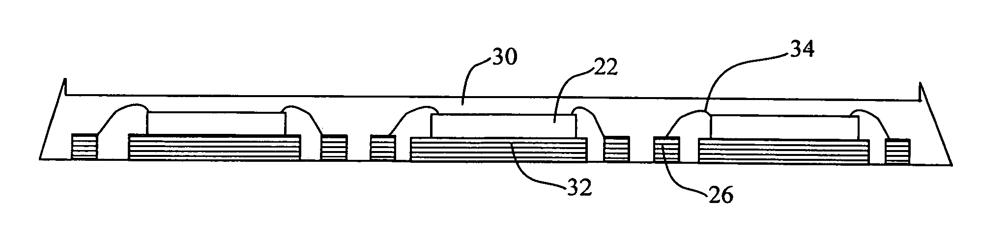
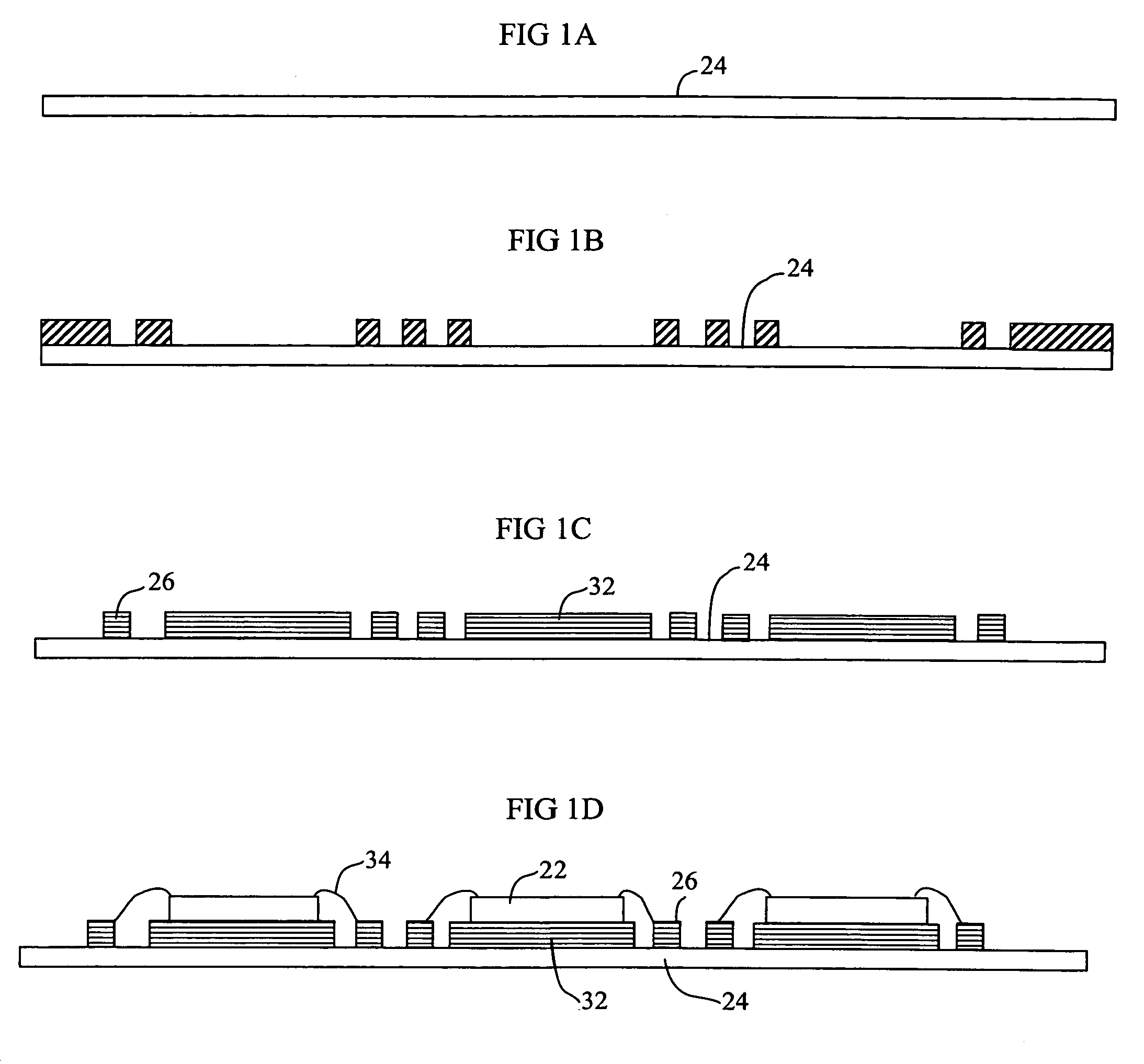
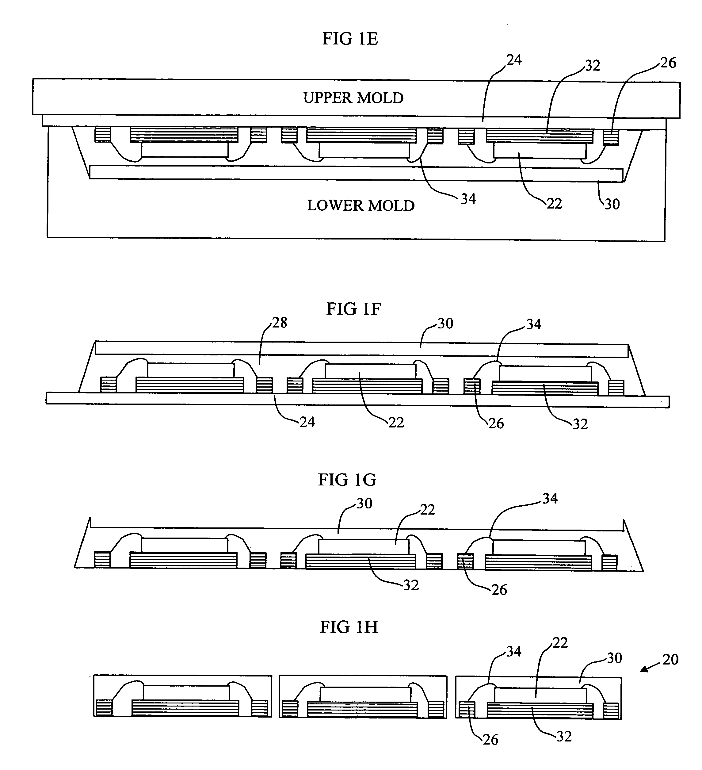
[0017]Referring to the figures, a process for fabricating an integrated circuit package will be described. The integrated circuit package is indicated generally by the numeral 20. The process includes mounting a semiconductor die 22 on a first surface of a metal carrier 24 and forming electrical connections between the semiconductor die 22 and ones of a plurality of contacts 26 on the metal carrier 24. Next, the semiconductor die 22 and the contacts 26 are molded in a molding material 28, between the metal carrier 24 and a metal strip 30. The metal carrier 24 and the metal strip 30 are etched away and the integrated circuit package 20 is singulated.
[0018]The process for fabricating the integrated circuit package 20 will now be described with particular reference to FIGS. 1A to 1H. For ease of illustration, the Figures show the processing steps for fabricating three integrated circuit packages 20. It will be understood, however, that the integrated circuit packages 20 are gang fabric...
PUM
 Abstract
Description
Claims
Application Information