Flip-chip semiconductor device

Inactive Publication Date: 2006-11-09
SILICONWARE PRECISION IND CO LTD
View PDF10 Cites 49 Cited by
  • Summary
  • Abstract
  • Description
  • Claims
  • Application Information

AI Technical Summary

Benefits of technology

[0012] In light of the above prior-art drawbacks, a primary objective of the present

Problems solved by technology

However, during the operation of the highly integrated, a large amount of heat is generated but cannot be effectively dissipated, because the chip is encapsulated by an encapsulant, which is made of a resin material with a low coefficient of thermal conductivity of 0.8 w/m-k.
Therefore, the performance and lifetime of the semiconductor device are adversely influenced and deteriorated.
Referring to the foregoing package structure, due to differences in the coefficient of thermal expansion (CTE) between the heat sink and the substrate, and between the heat sink and the chip, thermal stress may occur, resulting in warpage of the substrate and the overall package structure.
Thus, flatness of the substrate cannot be provided for mounting a plurality of solder balls.
Additionally, due to stress generated by the overall package structure, solder bumps mounted on the active surface of the flip-chip to electrically connect the chip to the substrate, may bear too much stress and be cracked.
However, after the beat sink is attached to the stiffener, mismatches of the coefficient of thermal expansion (CTE) still exist between vario

Method used


Image

  • Flip-chip semiconductor device
  • Flip-chip semiconductor device
  • Flip-chip semiconductor device

Examples


Embodiment Construction

[0028] The following embodiments are described in sufficient detail to enable those skilled in the art to make and use the invention. It is to be understood that other embodiments would be evident based on the present disclosure, and that proves or mechanical changes may be made without departing from the scope of the present invention.

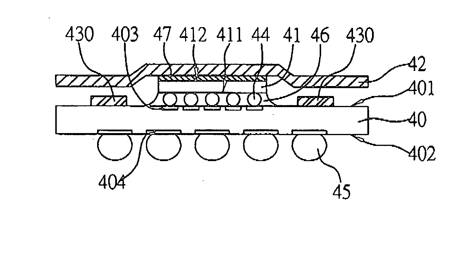
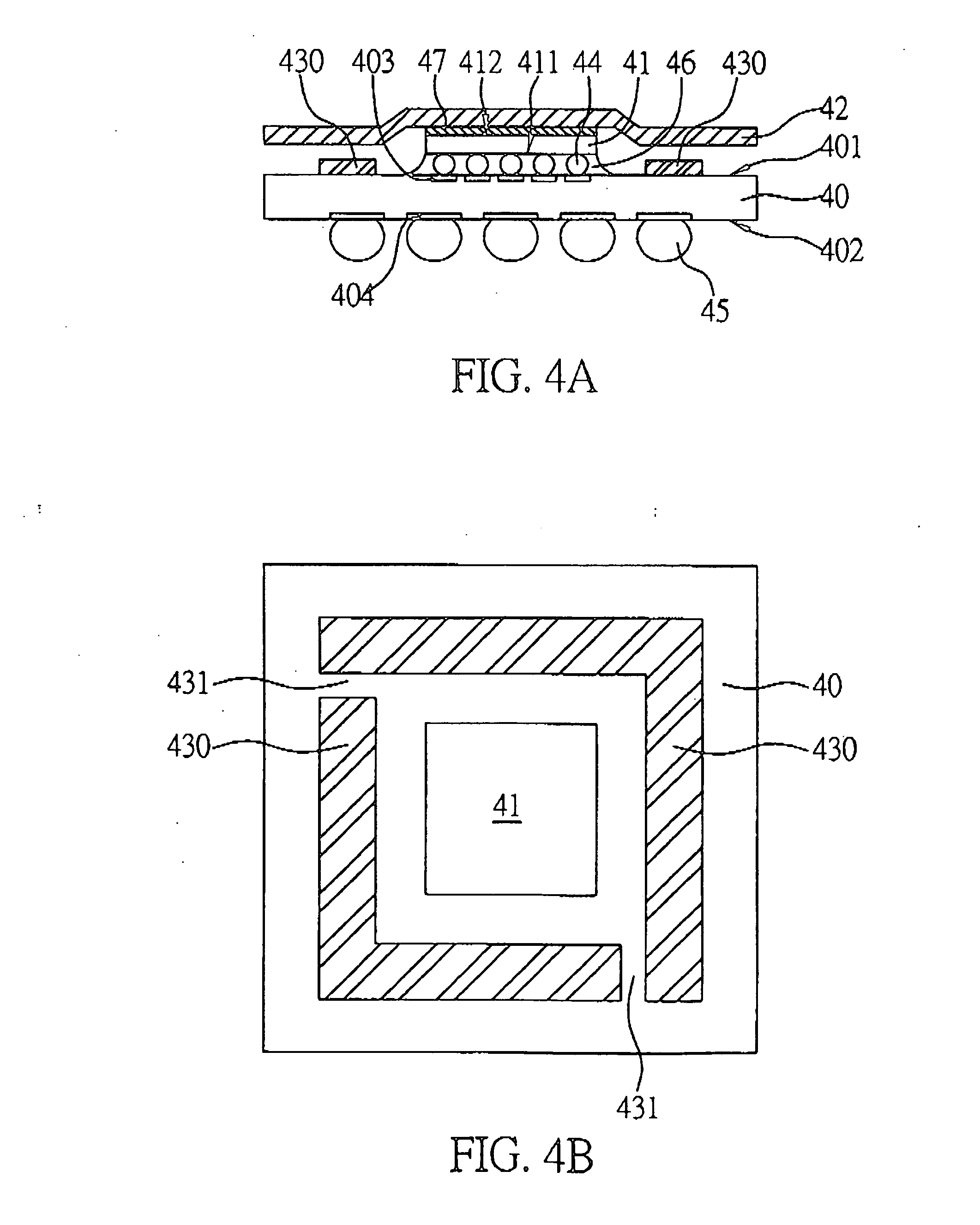
[0029]FIG. 4A is a cross-sectional view of a flip-chip semiconductor device according to the present invention, and FIG. 4B is a planar view of a flip-chip semiconductor device according to the present invention. The flip-chip semiconductor device comprises a substrate 40; a plurality of stiffeners 430 disposed at surrounding peripheral areas of the substrate 40, wherein a gap 431 is formed between each of the adjacent stiffeners 430; at least a semiconductor chip 41 mounted on an area of the substrate 40 surrounded by the stiffener 430, by flip-chip bonding technique; and a heat sink 42 attached to the semiconductor chip 41.

[0030] The substrate 40 ...


PUM


Abstract

A flip-chip semiconductor device is proposed, including a substrate, a plurality of stiffeners disposed at peripheral areas of the substrate, with a gap formed between each of the adjacent stiffeners; at least a semiconductor chip mounted on an area of the substrate surrounded by the stiffeners via flip-chip technique; and a beat sink attached to the semiconductor chip. By such arrangement, warpage of the semiconductor device may be prevented. As an opening is formed at an appropriate position of the stiffener structure, distortion of the stiffener may be avoided. Further, as the beat sink is not attached to the stiffener, solder bumps may be free from thermal stress due to mismatch in coefficient of thermal expansion between the heat sink and the substrate while preventing delamination of the heat sink caused by thermal stress.

Description

FIELD OF THE INVENTION [0001] The present invention relates to flip-chip semiconductor devices, and more particularly, to a flip-chip semiconductor package having a beat sink. BACKGROUND OF THE INVENTION [0002] Ball Grid Array (BGA) is an advanced semiconductor packaging technique, which is characterized in the use of a package substrate, having a front side thereof mounted with a semiconductor chip and a back side thereof mounted with a grid array of solder balls via self-alignment techniques. This thereby allows more input / output connections (I / O connections) to be provided on the same unit area of a semiconductor chip carrier to meet requirements of high integration of the semiconductor chip, such that an entire package unit can be electrically connected to an external device by the means of the solder ball. [0003] Further, a flip-chip semiconductor package is a packaging structure in which electrical connection is provided by flip-chip technique. In such semiconductor package, a...

Claims


Application Information

Patent Timeline
IPC IPC(8): H01L23/48
CPCH01L23/36H01L2924/01019H01L23/562H01L24/81H01L2224/16H01L2224/73253H01L2224/81801H01L2224/83102H01L2224/92125H01L2924/15311H01L2924/16152H01L2924/3511H01L23/49816H01L2924/00011H01L2924/00014H01L2224/0401
Inventor CHIU, SHIH-KUANGSUNG, MEI-YIHUANG, CHIEN-PINGHSIAO, CHENG-HSU
Owner SILICONWARE PRECISION IND CO LTD
Why Eureka
Try Eureka