Electronic component embedded substrate and method for manufacturing the same

a technology of embedded substrates and electronic components, which is applied in the association of printed electric components, printed circuit non-printed electric components, and semiconductor/solid-state device details, etc., can solve the problems of difficult to have electronic component embedded substrates b>1/b> in practical use, and difficulty in forming wiring patterns on conventional common printed wiring boards

Active Publication Date: 2006-02-02
SHINKO ELECTRIC IND CO LTD
View PDF9 Cites 51 Cited by
  • Summary
  • Abstract
  • Description
  • Claims
  • Application Information

AI Technical Summary

Benefits of technology

[0028] According to the above-described methods, an electronic component embedded substrate wherein a center plane of the substrate main body formed by the laminated first and sec

Problems solved by technology

However, it is difficult to form wiring patterns on conventional common printed wiring boards with the pitch as small as the pitch of the electrode pads formed on the semiconductor elements.
Therefore, the common print

Method used


Image

  • Electronic component embedded substrate and method for manufacturing the same
  • Electronic component embedded substrate and method for manufacturing the same
  • Electronic component embedded substrate and method for manufacturing the same

Examples


first embodiment

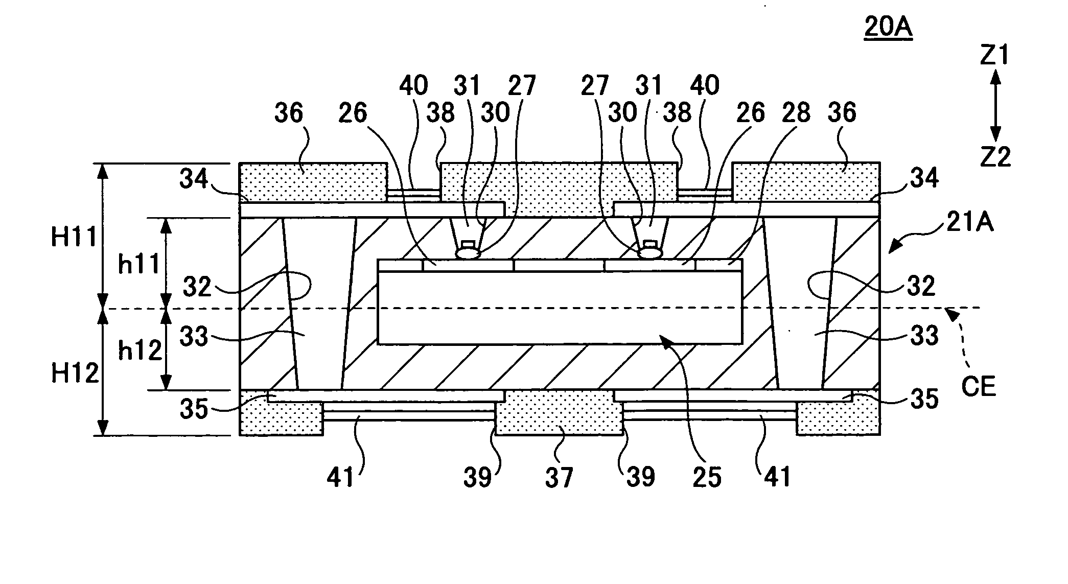
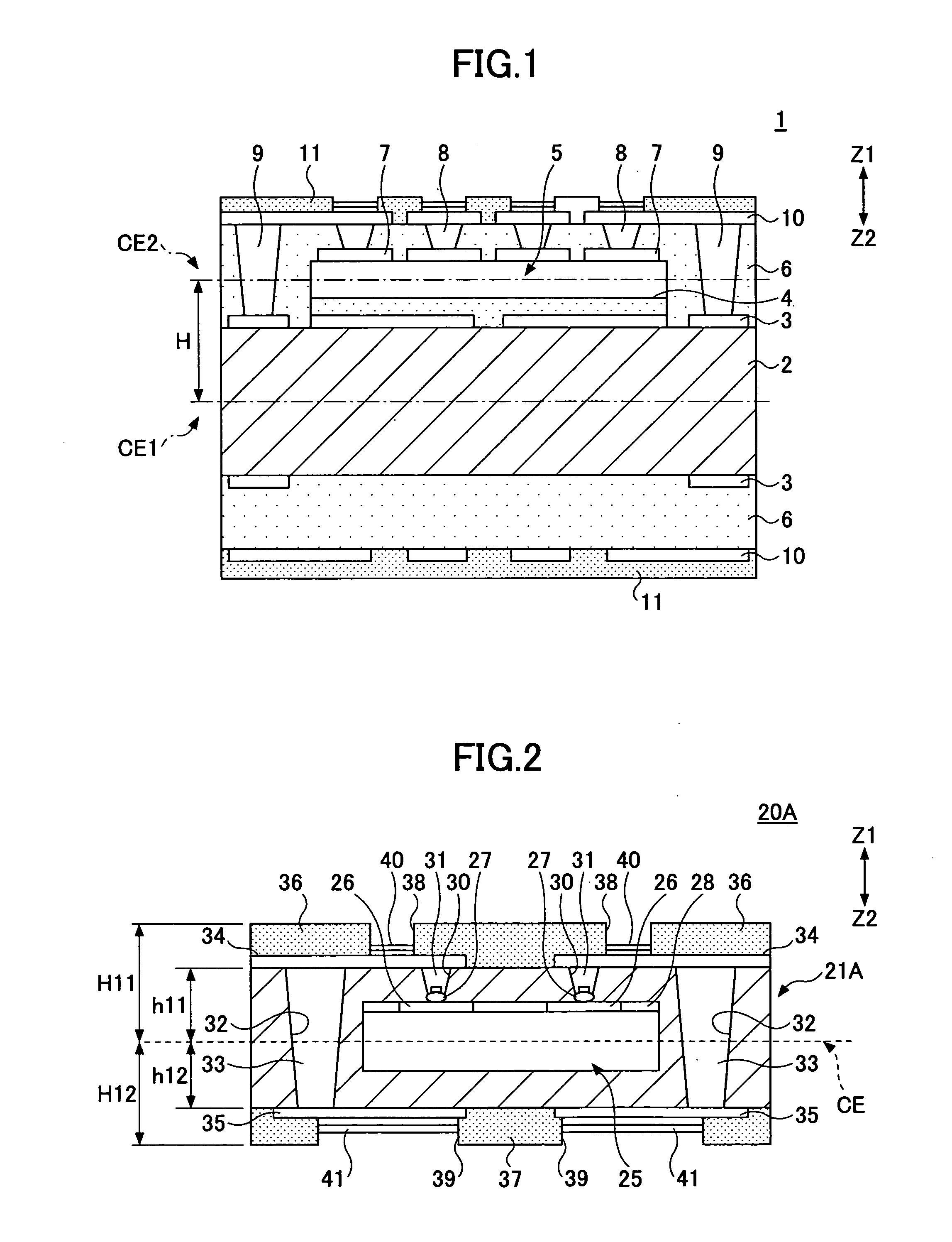
[0039]FIG. 2 is a cross-sectional view illustrating an electronic component embedded substrate 20A according to the present invention. The electronic component embedded substrate 20A has a very simple structure, comprising a substrate main body 21A and an electronic component 25.

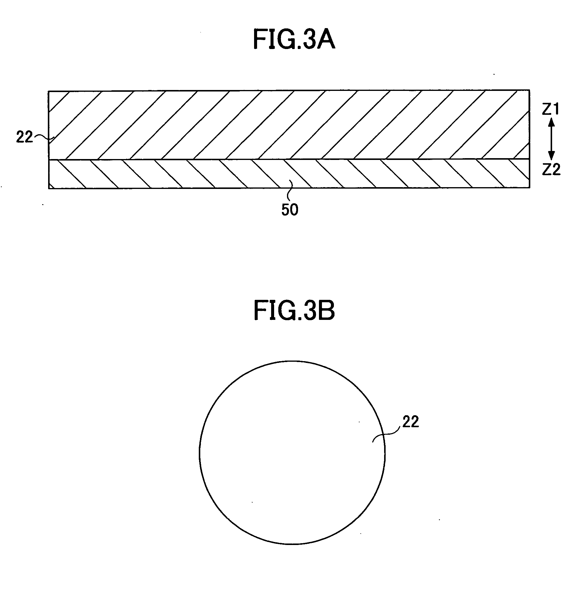
[0040] The substrate main body 21A has a laminated structure including first and second built-up layers 22 and 23 (as described below in detail), in which the electronic component 25 is embedded. The first and second built-up layers 22 and 23 are made of, for example, insulating epoxy resin.

[0041] In this embodiment, upper wires 34 and lower wires 35 are formed on an upper face and a lower face of the substrate main body 21A, respectively. With through vias 33 formed in through via holes 32 extending through the substrate main body 21, the upper wires 34 and the lower wires 35 are electrically connected to each other.

[0042] The electronic component 25 is, for example, a capacitor element or a semiconductor...

second embodiment

[0078] On the other hand, in the electronic component embedded substrate 20B only electrode stud bumps 27 are used for providing an electric connection between upper wires 34 and an electronic component 25, and stud bumps 42 are used for providing an electric connection between the upper wires 34 and lower wires 35.

[0079] Although there are differences as described above, the second embodiment is the same as the first embodiment in that a center plane of the electronic component 25 in a thickness direction (direction of arrows Z1 and Z2) and the center plane of the substrate main body 21B in the thickness direction (direction of arrows Z1 and Z2) are positioned to match each other, or are positioned on the same plane CE. Accordingly, a thickness h11 from the center plane CE to an upper face of the substrate main body 21B is equal to the thickness h12 from the center plane CE to a lower face of the substrate main body 21B (h11=h12).

[0080] Also, the center plane of the electronic co...

third embodiment

[0110] On the other hand, in the electronic component embedded substrate 20C of the third embodiment, a substrate main body 21C is configured to surround only lateral faces of an electronic component 25. In other words, the substrate main body 21C has a shape of a frame with a clearance area in the center in which the electronic component 25 is located.

[0111] The electronic component embedded substrate 20C is configured such that the electronic component 25 is embedded in the substrate main body 21C, but the upper and lower faces of the electronic component 25 are not covered with the substrate main body 21C. A part of upper wires 34 and a part of the lower wires 35 are formed directly on the electronic component 25.

[0112] Although there are differences as described above, the third embodiment is the same as the first and second embodiments in that a center plane of the electronic component 25 in a thickness direction (direction of arrows Z1 and Z2) and the center plane of the subs...


PUM

PropertyMeasurementUnit
Thicknessaaaaaaaaaa

Abstract

An electronic component embedded substrate and a method for manufacturing the substrate are disclosed. The electronic component embedded substrate includes a substrate main body and an electronic component embedded in the substrate main body. The center plane of the electronic component in the thickness direction thereof and the center plane of the substrate main body in the thickness direction thereof generally match each other.

Description

BACKGROUND OF THE INVENTION [0001] 1. Field of the Invention [0002] The present invention relates to an electronic component embedded substrate and a method for manufacturing the same, and particularly relates to an electronic component embedded substrate wherein an electronic component is embedded in a substrate main body and a method for manufacturing the same. [0003] 2. Description of the Related Art [0004] In these years, as semiconductor elements with higher operating frequency have been mounted on semiconductor devices, stabilization of the power supply voltage to the semiconductor elements is becoming necessary. To meet such a need, an electronic component embedded substrate is proposed wherein an electronic component (e.g. capacitor element) is embedded in a semiconductor substrate on which a semiconductor element is mounded. [0005] In the meantime, with the increase of mounting density of semiconductor elements, the pitch of electrode pads formed on the semiconductor elemen...

Claims


Application Information

Patent Timeline
IPC IPC(8): H05K1/03
CPCH01L23/5389Y10T29/49126H01L24/82H01L2221/68345H01L2224/1134H01L2224/24226H01L2224/73267H01L2224/82047H01L2924/01029H01L2924/01058H01L2924/01078H01L2924/01079H01L2924/19041H05K1/185H05K3/4602H01L2224/13099H01L2924/00013H01L2924/01005H01L2924/01006H01L2924/01033H01L2924/014H01L24/24Y10T29/49146H01L2224/0557H01L2224/05573H01L2924/00014H01L2224/05571H01L2224/0554H01L2924/3511H01L2224/04105H01L2224/05599H01L2224/0555H01L2224/0556H05K1/18H05K3/30
Inventor SUNOHARA, MASAHIROHIGASHI, MITSUTOSHIMURAYAMA, KEIKATO, HIROYUKI
Owner SHINKO ELECTRIC IND CO LTD
Why Eureka
Try Eureka