Multilayered wiring substrate and method of manufacturing the same

a wiring substrate and multi-layer technology, applied in the direction of printed circuit manufacturing, printed circuit aspects, high current circuit adaptations, etc., can solve the problems of reducing the size of electronic devices, unable to achieve a higher density of the overall multi-layer wiring substrate, and difficulty in miniaturizing through holes, so as to reduce the thickness and suppress the generation of warpage

Inactive Publication Date: 2007-03-15
SHINKO ELECTRIC IND CO LTD
View PDF15 Cites 54 Cited by
  • Summary
  • Abstract
  • Description
  • Claims
  • Application Information

AI Technical Summary

Benefits of technology

[0008] Embodiments of the present invention provide a multilayered wiring substrate capable of suppressing generation of a warpage while seeking a reduction in thickness and a method of manufacturing the same.
[0010] According to the first aspect of the present invention, the reinforcing wiring layer whose thickness is set to 35 to 150 μm can execute two functions of a function as the wiring layer and a function of suppressing generation of a warpage. Therefore, generation of a warpage can be suppressed without use of other reinforcing member, or the like, and also generation of the warpage can be suppressed while seeking a reduction in thickness of the multilayered wiring substrate.
[0012] According to the present invention, a warpage generated in the multilayered wiring substrate can be prevented effectively.
[0016] According to the second aspect of the present invention, because the thickness of the reinforcing wiring layer is set to 35 to 150 μm, which is thicker than the normal thickness, in the step that is always applied to form the wiring in the steps of manufacturing the multilayered wiring substrate, the warpage of the multilayered wiring substrate can be suppressed. Therefore, there is no need to change the manufacturing steps and the manufacturing equipment, and thus the multilayered wiring substrate a warpage of which is not generated can be manufactured at a low cost.
[0017] Various implementations may include one or more the following advantages. For example, generation of the warpage of the multilayered wiring substrate can be suppressed while seeking a reduction in thickness of the substrate.

Problems solved by technology

However, since this multilayered wiring substrate has the core layer in the inside, there exists such a problem that it is difficult to miniaturize through holes formed in the core layer and the higher density of the overall multilayered wiring substrate cannot be achieved.
Also, there existed such a problem that, because the core layer is provided, the multilayered wiring substrate becomes thick inevitably and thus a reduction in size of the electronic device is hindered.
However, when the core layer acting as the reinforcing member is merely removed, there is such a problem that a warpage of the multilayered wiring substrate is generated due to a difference in thermal expansion between the insulating layer made of a resin and the wiring layer made of metal, and the like.
In case such warpage is generated, the semiconductor element, and the like cannot be properly mounted on the multilayered wiring substrate in the mounting step, and also it is difficult to package the semiconductor package into the packaging substrate.
Also, an interlayer connection of the wiring layers cannot be surely built up in the multilayered wiring substrate, and it is feared that the reliability of the multilayered wiring substrate is also lowered.

Method used


Image

  • Multilayered wiring substrate and method of manufacturing the same
  • Multilayered wiring substrate and method of manufacturing the same
  • Multilayered wiring substrate and method of manufacturing the same

Examples


Embodiment Construction

[0033] Next, a best mode for carrying out the invention will be explained in line with the drawings hereinafter.

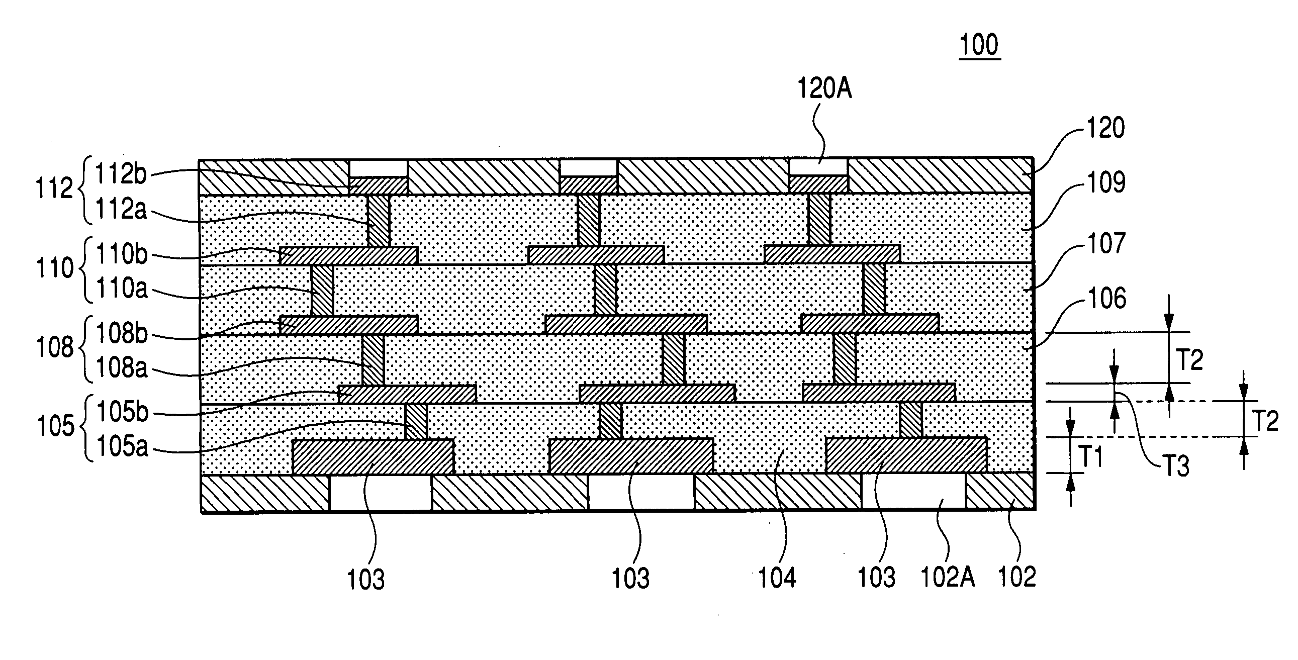
[0034]FIG. 1 shows a multilayered wiring substrate 100 as an embodiment of the present invention. As shown in FIG. 1, in the present embodiment, explanation will be made hereunder while taking the multilayered wiring substrate 100 having a five-layered structure as an example. However, the application of the invention of this application is not limited to the five-layered structure, and the present invention can be applied widely to the multilayered wiring substrate 100 having various numbers of layers.

[0035] The multilayered wiring substrate 100 is constructed by stacking reinforcing wiring layers 103, a first insulating layer 104, wirings 105, a second insulating layer 106, wirings 108, a third insulating layer 107, wirings 110, a fourth insulating layer 109, and wirings 112, when classified roughly, from the lower layer to the upper layer sequentially. Also, a solder ...


PUM


Abstract

A multilayered wiring substrate constructed by staking a wiring layer 105, 108, 110, 112 and an insulating layer 104, 106, 107, 109 in predetermined number, which includes a reinforcing wiring layer 103 whose thickness is 35 to 150 μm is arranged in one layer or plural layers.

Description

TECHNICAL FIELD [0001] The present disclosure relates to a multilayered wiring substrate and a method of manufacturing the same and, more particularly, a multilayered wiring substrate to which a reinforcing means is provided to prevent a warpage and a method of manufacturing the same. RELATED ART [0002] The improvements in performance and size of the electronic device using the semiconductor device such as the semiconductor chip, or the like are proceeding nowadays. Accordingly, the integration density of the semiconductor device is increased and also a tendency to grow multiple pins and a downsizing is sought. As the substrate on which the semiconductor device whose number of pins are increased and whose size is reduced is mounted, the multilayered wiring substrate using the built-up method is provided. [0003] The multilayered wiring substrate of this type is constructed such that the reinforcing member such as the woven glass fabric copper-clad laminate, or the like is used as the...

Claims


Application Information

Patent Timeline
Patent Type & Authority Applications(United States)
IPC IPC(8): H01L23/04H01L21/44
CPCH01L23/49822H01L2224/16H01L2924/01078H01L2924/15174H01L2924/15311H05K1/0265H01L2224/16235H05K3/423H05K3/4682H05K2201/0352H05K2201/09736H05K2203/0733H05K3/205H05K3/46
Inventor NAKAMURA, JUNICHINAGATA, KINJI
Owner SHINKO ELECTRIC IND CO LTD
Why Eureka
Try Eureka