Digital imbalance correction method and device in a receiver for multi-carrier applications

a multi-carrier, digital imbalance technology, applied in the direction of modulation, amplitude demodulation, transmission monitoring, etc., can solve the problems of amplitude (gain) and phase imbalance, performance degradation, and reduce the signal-to-noise ratio s/n of the receiver, so as to avoid the very tedious frequency planning process, the effect of complexity and cos

Inactive Publication Date: 2008-05-20
NOKIA CORP
View PDF15 Cites 23 Cited by
  • Summary
  • Abstract
  • Description
  • Claims
  • Application Information

AI Technical Summary

Benefits of technology

[0025]Consequently, it is an object of the present invention to provide an improved method and device for digital imbalance correction which enables the realization of direct conversion for multi-carrier signals.
[0050]By virtue of the present invention, basically the following advantages can be achieved:
[0054]Thus, the present invention provides a way to estimate and / or calculate phase and amplitude errors and / or imbalance of an analogue IQ-demodulator in a receiver using digital processing. This enables the use of direct conversion architectures in multi-carrier receivers. The use of the received antenna signal as such enables to estimate the imbalance in the modulator, without needing a special test signal.
[0055]There seem to be no other applicable methods for estimating IQ imbalance in analog IQ modulators for multi-carrier receivers. If IQ balance can be estimated and compensated properly, it enables a direct conversion architecture in which the received signals are converted to the digital domain at baseband frequencies. This results into minimum complexity of the receiver and the easiest requirements for the A-to-D converters. The direct conversion architecture also avoids the very tedious frequency planning process in the receiver, because no intermediate frequencies are needed.

Problems solved by technology

One of the key impairments of this architecture resides in an amplitude (gain) and phase imbalance of the two (or multiple) signal branches in the receiver.
In a single carrier receiver (RX) this I / Q-imbalance reduces the signal-to-noise ratio S / N of the receiver and causes performance degradation.
In the case of multi-carrier reception, however, amplitude and phase imbalance of the two branches (i.e. I and Q branch) cause interference of the channels located at equal frequency differences above and below the frequency of the local oscillator 6.
Currently available analog-to-digital converters (ADCs) are, however, not sufficient and immense effort is spent by various manufactures to overcome this problem.A double conversion to a low IF and low-pass sampling.
This, however, requires enormous linearity of the RF stages.
Although it seems to be feasible, it is associated with rather high implementation costs.
Furthermore, the double IF solution is prone to spurious responses and requires different IF frequencies for different RF bands.
However, most of these methods share the problem of being unable to compensate for amplitude and phase mismatches which depend on frequency and / or time.
Furthermore, most of the proposed estimation techniques are based on known test or calibration signals, thereby complicating their use during the normal receiver operation.
Consequently, the drawbacks of the known methods are one or a combination of the following:Not able to compensate frequency dependent mismatchesNot able to compensate time dependent mismatchesNeed for test or calibration signals.
However, in order to function properly, the assumed frequency dependency model has to be correct.
Otherwise, the desired result can not be obtained.
However, the estimation of time dependency is also a problem in case of fast varying signals, such as in the GSM system.
In summary, direct conversion of a multi-carrier signal, however, is currently not feasible for cellular applications.

Method used


Image

  • Digital imbalance correction method and device in a receiver for multi-carrier applications
  • Digital imbalance correction method and device in a receiver for multi-carrier applications
  • Digital imbalance correction method and device in a receiver for multi-carrier applications

Examples


Embodiment Construction

[0064]The present invention will subsequently be described in detail with reference to the accompanying drawings.

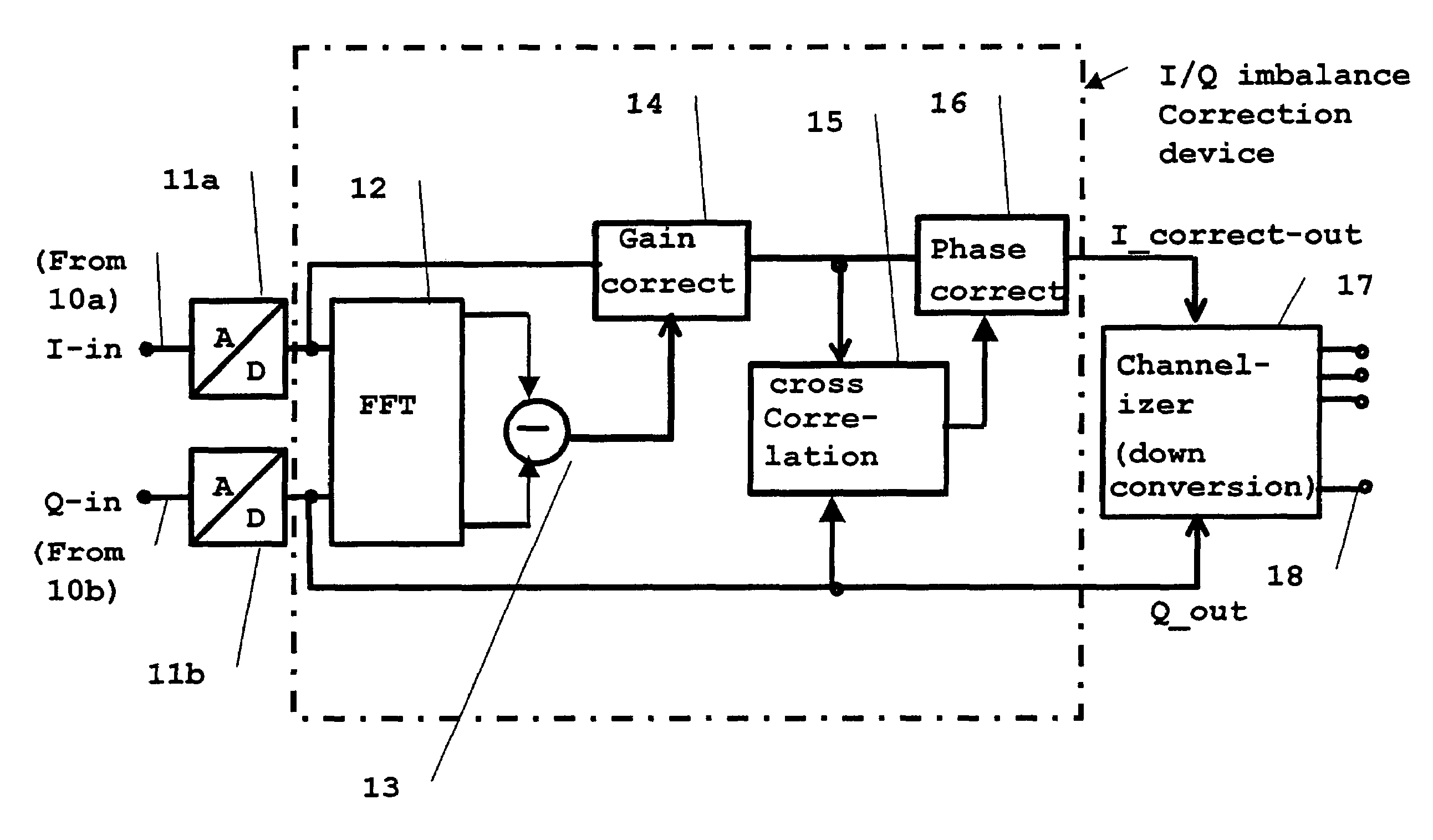
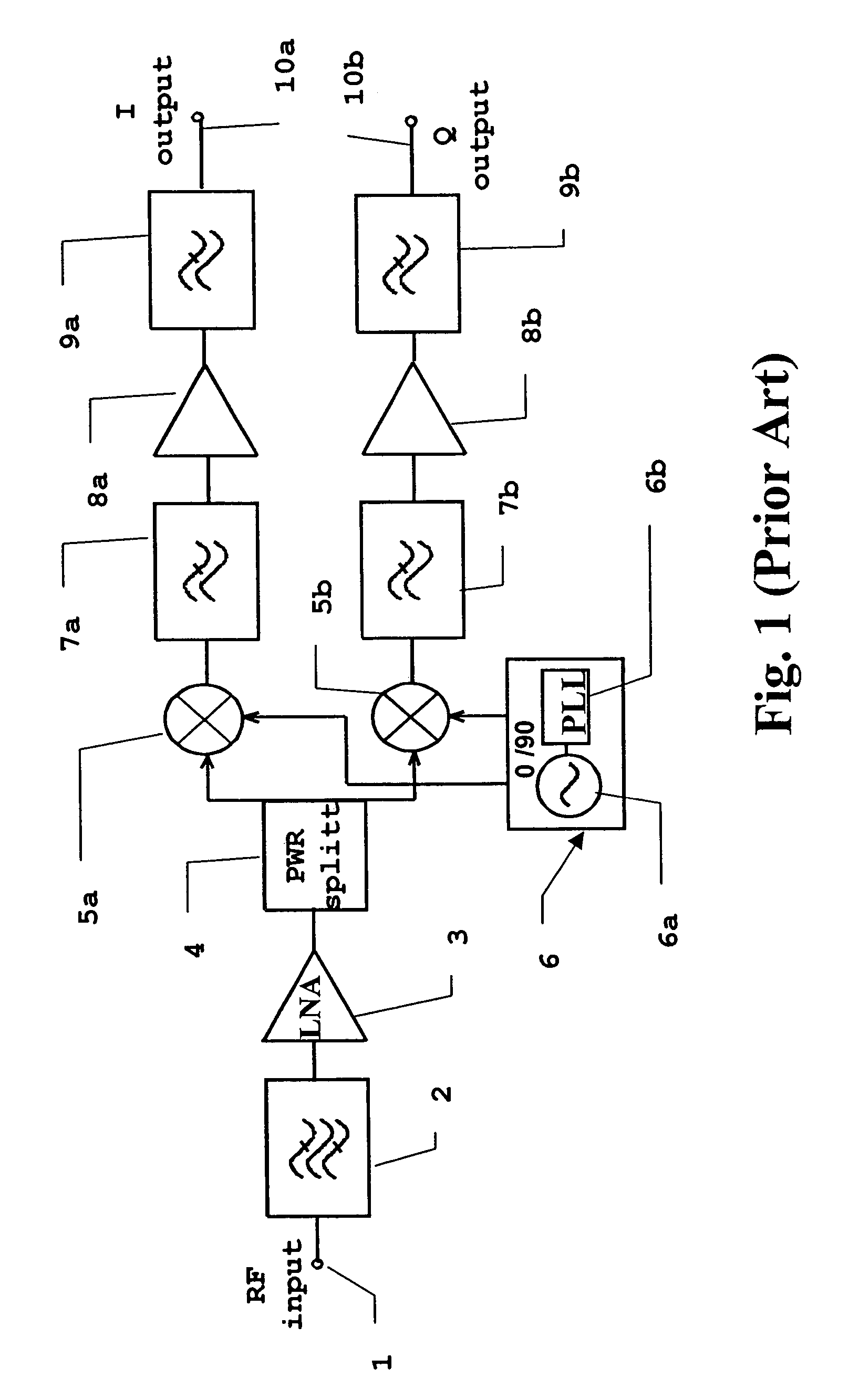
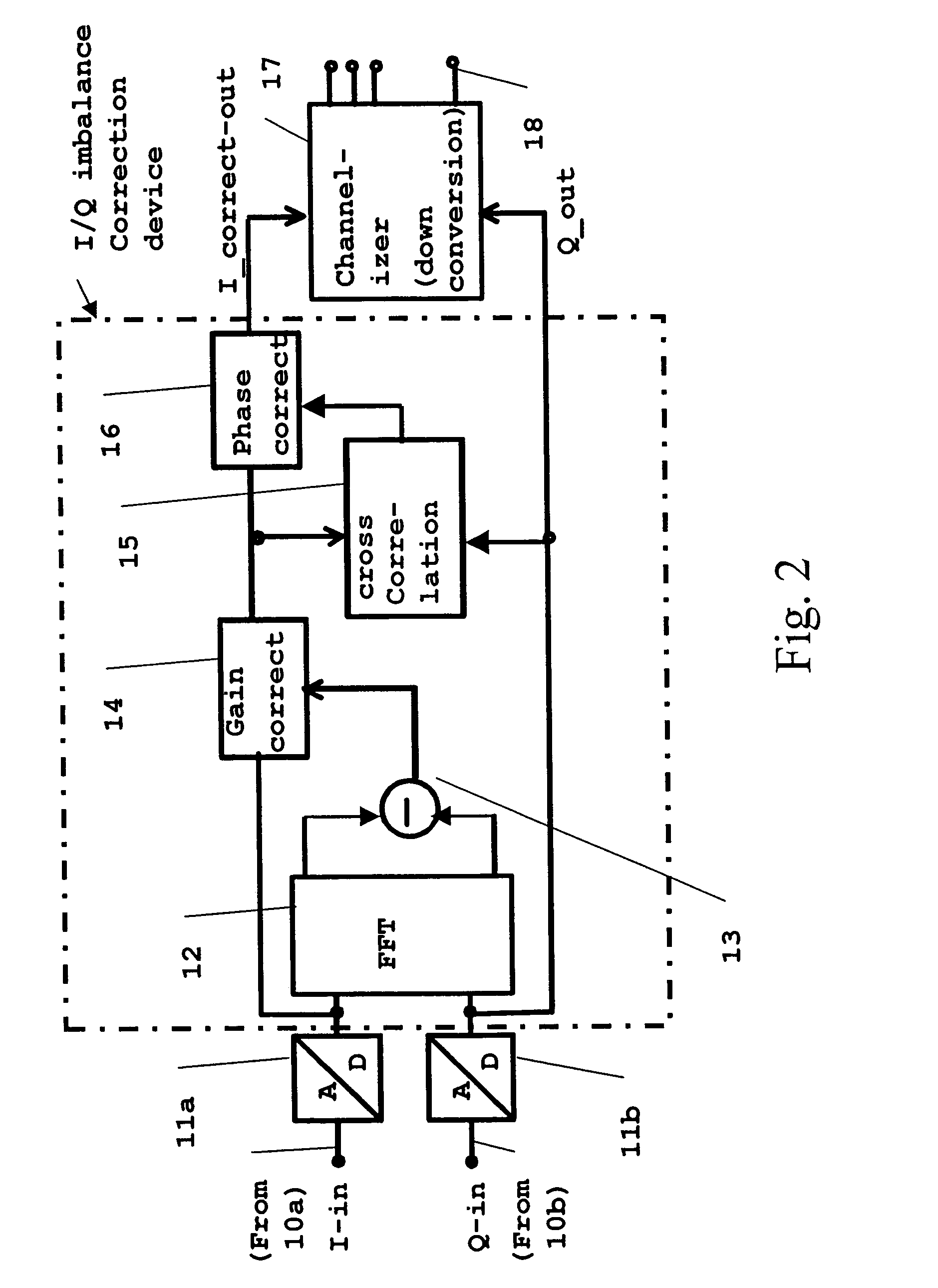
[0065]FIG. 2 shows an embodiment of the digital error correction device according to the present invention. The error correction device may be used as a subsequent stage following the analog part of an I / Q conversion receiver as for example shown in FIG. 1. Nevertheless, it may be used as a subsequent stage for imbalance / error correction following also other kinds of multi-branch receivers as long as they output signal components converted with oscillator signals of multiple phases. For example, the imbalance (error) correction device may also be connected to the output of a double quadrature receiver or tri-phase receiver. Firstly, the structure of the embodiment shown in FIG. 2 will be described. As shown, the I / Q outputs of the FIG. 1 arrangement are input as signals I-in and Q-in at respective input terminals. Each signal I and Q, respectively, is supplied to a corres...


PUM


Abstract

A digital imbalance correction device and method are provided including an input unit to receive first input signals. A time-to-frequency-domain-transformer performs a transformation of the first input signals from time-domain into frequency-domain. A subtractor receives second input signals and outputs a gain difference as a function of frequency at its output. A cross-correlator receives third input signals based on the input signals, and outputs a cross-correlation of the third input signals. A gain corrector receives a fourth input signal based the associated first input signal. A gain of the fourth input signal is corrected based on the power difference spectrum. A phase corrector receives a fifth input signal based the associated first input signal. A phase of the fifth input signal is corrected based on the cross-correlation output, such that the phase of the fifth input signal is in quadrature relation to the other one of the first input signals.

Description

BACKGROUND OF THE INVENTION[0001]1. Field of the Invention[0002]The present invention relates to a digital imbalance correction method and device. In particular, the present invention relates to such a device adapted for use in a receiver designed for multi-carrier applications.[0003]2. Description of the Related Art[0004]With the recent progress in telecommunications, receivers tend to be designed for so-called multi-carrier applications in order to be able to receive signals composed of multiple carriers, each carrier originating from a different transmitter. For example, such applications are likely to occur in connection with e.g. frequency diversity scenarios.[0005]This invention relates to such broadband dual (or multi-) branch receivers for such multi-carrier applications. A broadband dual (or multi-) branch converter is used to convert the complete RF band (Radio Frequency) of interest including multiple channels / carriers to a low pass limited frequency band. This low-pass l...

Claims


Application Information

Patent Timeline
Patent Type & Authority Patents(United States)
IPC IPC(8): H04B1/69H04B1/66H03D3/00H04L27/26
CPCH03D3/009H04L27/265H04L27/26524
Inventor SCHECK, HANS-OTTO
Owner NOKIA CORP
Why Eureka
Try Eureka