Method and apparatus for applying charged particle beam

a technology of charged particles and beams, applied in the field of methods and apparatus for applying charged particle beams, can solve the problems of speed of processing subject, i, accuracy improvement, etc., and achieve the effect of improving the throughput of the charging particle beam applying apparatus and facilitating the position adjustment of the crossover

Active Publication Date: 2008-05-27
HITACHI HIGH-TECH CORP +1
View PDF4 Cites 26 Cited by
  • Summary
  • Abstract
  • Description
  • Claims
  • Application Information

AI Technical Summary

Benefits of technology

[0021]Furthermore, a ratio in size between the source crossover 106 and the intermediate image of the crossover converged at the height of the blanker array 112 is determined by an inverse ratio between a distance from the source crossover 106 to a main surface of the condenser lens 107 and a distance from a main surface of the lens array 109 to the blanker array 112. Therefore, if the front focal plane of the condenser lens 107 is aligned with the displaced source crossover 106, the size of the intermediate image of the crossover converged at the height of the blanker array 112 may be changed. This means to vary the size of each beam reaching onto the test sample, so that such variation affects drawing accuracy.
[0025]Therefore, an object of the present invention is to provide, in a charged particle beam applying apparatus such as an electron beam lithography system, a technology that can facilitate a positional adjustment of a crossover and improve throughput of the apparatus.
[0029]Note that since the end face is an obstacle on the beam path at a time of drawing, the present invention is configured to be removable from a beam axis without deteriorating a near vacuum state.
[0030]Also, the present invention is characterized by, for a plurality of electron beams, measuring a relative position with respect to the corresponding lens or blanker and by comparing the measured relative position with a relative position at a time of initial adjustment. That is, a change in focal length of the condenser lens is monitored, and adjustment is made if the change in focal length exceeds a tolerance. Thereby, the parallelism of the electron beams with which the aperture array is irradiated can be appropriately managed.
[0032]The positional adjustment of the crossover is facilitated and the throughput of the charged particle beam applying apparatus can be improved.

Problems solved by technology

In these semiconductor manufacturing devices applying electron beams, it is an important problem that the speed of processing the subject, i.e., throughput is improved along with accuracy.

Method used


Image

  • Method and apparatus for applying charged particle beam
  • Method and apparatus for applying charged particle beam
  • Method and apparatus for applying charged particle beam

Examples


first embodiment

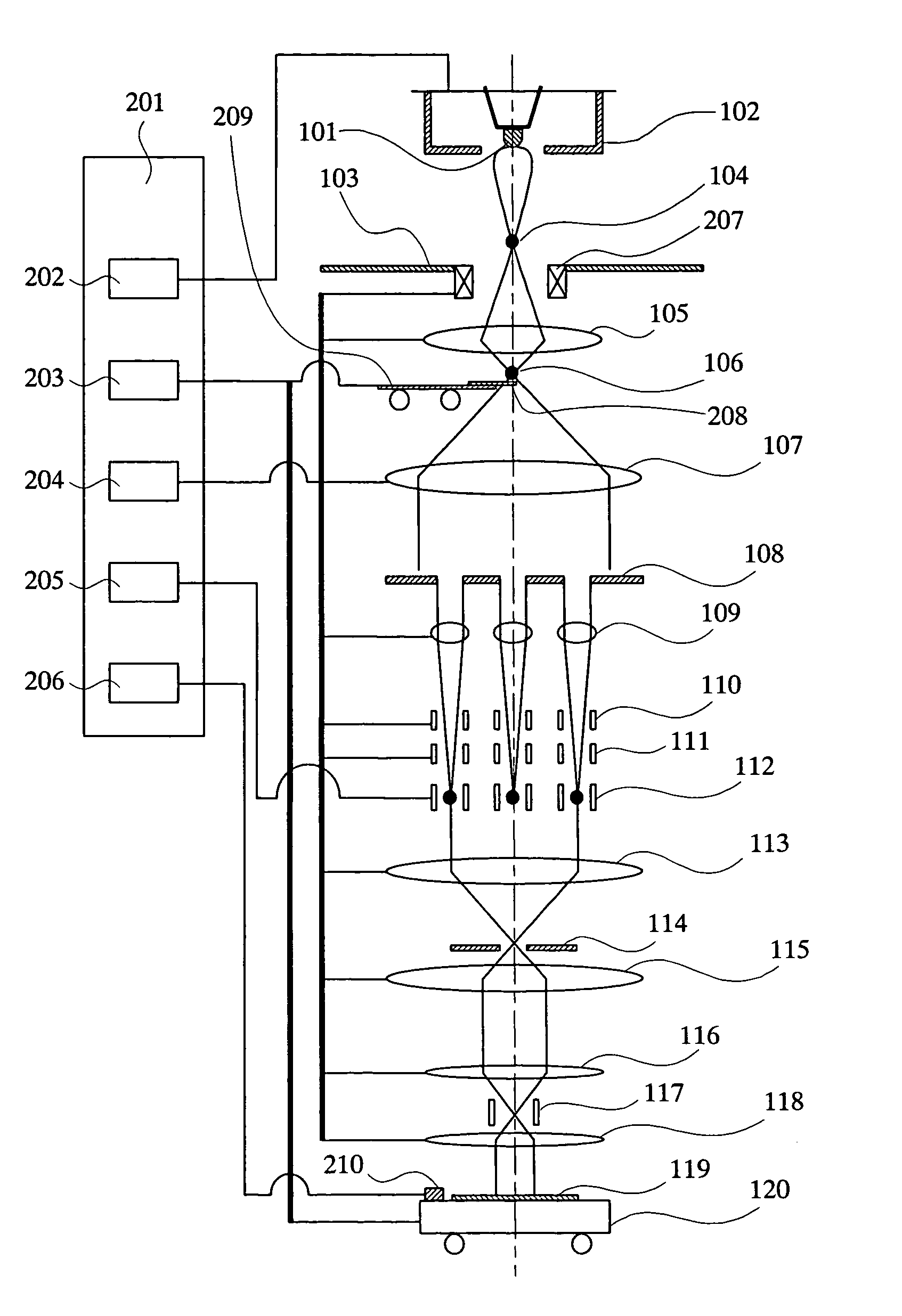
[0051]FIG. 1 is a view showing a schematic structure of a multibeam electron-beam lithography system according to a first embodiment of the present invention. Members shown in FIG. 1 and having the same reference numerals as those in FIG. 13 indicate the same members as those in FIG. 13.

[0052]Firstly, with reference to FIG. 1, one example of the multibeam electron-beam lithography system according to the first embodiment will be described. The multibeam electron-beam lithography system according to the first embodiment includes, for example, an electron gun composed of a cathode 101, a Wehnelt cylinder 102, and others; an anode 103; an aligner 207; a source forming lens 105; a movable stage 209 equipped with a crossover regulation edge 208; a condenser lens 107; an aperture array 108; a lens array 109; deflector arrays 110 and 111; a blanker array 112; reducing glasses 113 and 115; a blanking aperture 114; objective lenses 116 and 118; a deflector 117; a stage 120; a Faraday cup 210...

second embodiment

[0070]FIG. 4 is a view showing a schematic structure of a multibeam electron-beam lithography system according to a second embodiment of the present invention. Components shown in FIG. 4 and having the same reference numerals as those in FIGS. 1 and 13 are identical to those in FIGS. 1 and 13.

[0071]In the second embodiment, two-stage electromagnetic lenses, that is, a first source forming lens 501 and a second source forming lens 502 are provided between the front focal plane of the crossover 104 and the front focal plane of the condenser lens 107. By using these lenses, the crossover formed by the electron gun is reduced to form an image on the front focal plane of the condenser lens 107. Since the first source forming lens 501 and the second source forming lens 502 are used together as a zoom lens, the crossover is reduced with an arbitrary magnification to form an image relative to the source crossover 106 on the front focal plane of the condenser lens 107.

[0072]Therefore, in the...

third embodiment

[0091]In the above first and second embodiments, a single crossover regulation edge regulating the height of the crossover has been used. By contrast, in a third embodiment, a plurality of crossover regulation edges are used.

[0092]FIG. 7 is a view showing a structure of crossover regulation edges for use in the third embodiment. The reference numerals “801”, “802”, and “803” denote crossover regulation edges with different heights supported by one movable stage 804. In the third embodiment, in place of the crossover regulation edge 208 and the movable stage 209 as shown in FIGS. 1 and 4, the crossover regulation edges 801, 802, and 803 are placed between the crossover 104 and the condenser lens 107.

[0093]In the present embodiment, through the same method as that according to the first embodiment, a condition under which an intermediate image of the crossover is formed for each of three crossover regulation edges 801, 802, and 803 is obtained. That is, a current for the source formin...


PUM


Abstract

In a charged particle beam applying apparatus such as an electron beams lithography system, there is a technology that facilitates positional adjustment of a crossover and improves throughput of the apparatus. A front focal plane of a condenser lens is provided with a sharp end face (crossover regulation edge) for regulating the height of the crossover on a beam axis. By using the crossover regulation edge to measure the shape of an electron beam, the shape of the beam on the front focal plane of the condenser lens can be always checked even if the height of the crossover formed by an electron gun or the resistance of a source forming lens is changed.

Description

CROSS-REFERENCE TO REIATED APPLICATION[0001]The present application claims priority from Japanese patent application No. JP 2005-188345 filed on Jun. 28, 2005, the content of which is hereby incorporated by reference into this application.BACKGROUND OF THE INVENTION[0002]The present invention relates to a method and apparatus for applying charged particle beams and, particularly, to a technology effectively applied to a high-speed and high-accuracy apparatus for applying charged particle beams, which is used for semiconductor manufacturing devices and semiconductor inspection apparatuses.[0003]Examples of technologies studied by the present inventors are as follows in a charged electron beam applied technology for use in a semiconductor manufacturing process.[0004]In the semiconductor manufacturing process, an electron beam lithography system is used for drawing a desired circuit pattern on a wafer or mask as a subject. Also, electron microscopes, electron-beam inspection devices, a...

Claims


Application Information

Patent Timeline
Patent Type & Authority Patents(United States)
IPC IPC(8): H01J3/14G21K1/08
CPCB82Y10/00B82Y40/00H01J37/1471H01J37/304H01J37/3174H01J2237/0458H01J2237/1501H01J2237/31774H01J2237/31776
Inventor TANIMOTO, SAYAKASOHDA, YASUNARISOMEDA, YASUHIROHOSODA, MASAKI
Owner HITACHI HIGH-TECH CORP
Why Eureka
Try Eureka