Snubber circuit for a power converter

a power converter and circuit technology, applied in the direction of electric variable regulation, process and machine control, instruments, etc., can solve the problems of low efficiency power conversion, voltage across capacitor b, inability to control, etc., to reduce switch conduction and turn on losses, easy control, and small cost

Inactive Publication Date: 2008-06-10
ASTEC INT LTD
View PDF21 Cites 214 Cited by
  • Summary
  • Abstract
  • Description
  • Claims
  • Application Information

AI Technical Summary

Benefits of technology

[0008]An advantage of the present invention is that the voltage across the resonant capacitor is controlled such that, after the resonant action, it is higher than before. The voltage in the resonant capacitor circuit according to the present invention is well defined and can be easily controlled at turn ON by adjusting the turns ratio of the two inductor windings.
[0009]Another advantage of the present invention is that the drain voltage of the main MOSFET switch is clamped well to the output voltage so as to enable the use of much lower voltage and Rdson MOSFET switches that are smaller and less costly which reduces switch conduction and turn on losses.
[0010]Another advantage of the present invention is that it reduces electromagnetic interference (EMI) since the size of the spike generated at the drain of MOSFET is reduced.
[0011]Broadly stated, the present invention provides a power converter having first and second input terminals where an input voltage is provided and first and second output terminals where the output DC voltage is provided, the converter comprising a first inductor having one end connected to the first input terminal; a boost diode connected in series between the first inductor and the first output terminal; a first capacitor coupled across the first output terminal and the second output terminal; a switch alternately switched on and off as a function of a control signal for controlling current through the first inductor; the switch is connected between the first input terminal and a first node at the junction of the first winding and the boost diode; and a snubber circuit comprising a series combination of a second inductor magnetically coupled to said first inductor, a second diode and a third diode connected between the output terminals; and a resonant capacitor connected in series with the third diode between the first node and the first output terminal.

Problems solved by technology

Drawbacks of such conventional boost converter circuits include the creation of switch voltage and current stresses, which result in low efficiency power conversion.
A drawback of the circuit in FIG. 2 is that the voltage across capacitor 22 cannot be controlled at turn on and so, after the half resonant period, the reverse voltage is less than before.
Consequently, the performance of the circuit in FIG. 2 is not suitable, particularly in high power applications.
Thus, although an improvement over converter 10 of FIG. 1, converter 20 has the similar drawback of having an unacceptably high voltage spike (>Vout) at the drain of MOSFET 14 for high current applications so as to require higher voltage rated MOSFETS with higher Rdson and corresponding higher conduction losses.

Method used


Image

  • Snubber circuit for a power converter
  • Snubber circuit for a power converter
  • Snubber circuit for a power converter

Examples


Embodiment Construction

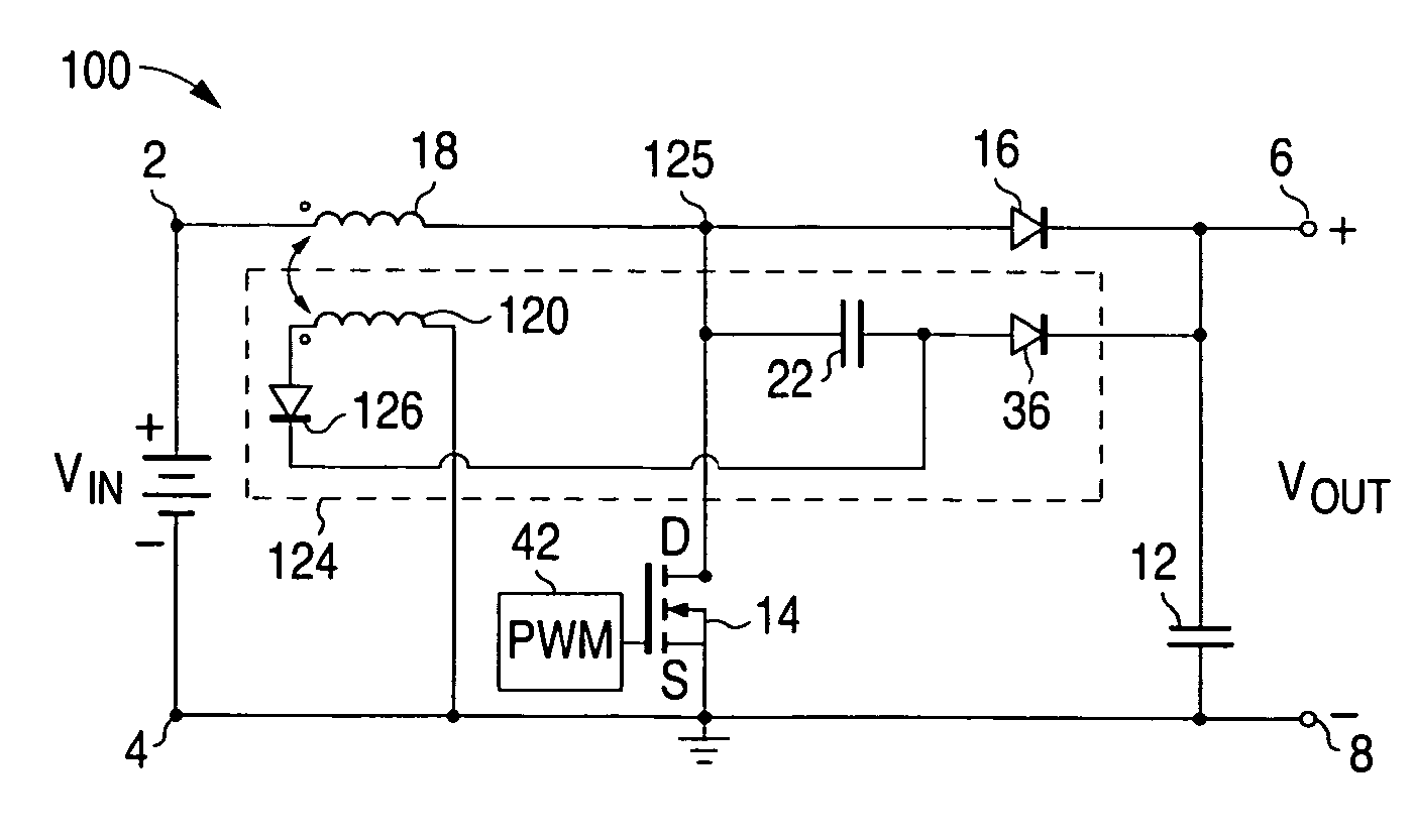
[0023]The circuit and boost converter topology according to the present invention provides a resonant snubber for reducing the voltage spike developed in the drain of the main MOSFET switch caused by the large current pulse and the parasitic inductance.

[0024]FIG. 3 is a schematic diagram of a preferred embodiment of the snubber circuit 124 and boost converter according to present invention. Boost converter 100 comprises a snubber circuit 124 added to the boost converter 10 of FIG. 1. The snubber circuit 124 is designed to suppress the spike generated at the drain of MOSFET 14 caused by the large current pulse and the leakage (parasitic) inductance in the circuit when MOSFET 14 is turned off and to transfer this energy to the output. The snubber circuit 124 includes a series combination of a capacitor 22 and a diode 36 connected across s diode 16. The capacitor 22 is connected at one end to the junction of the inductor 18 and the diode 16 at a node 125. Snubber circuit 124 includes a...


PUM


Abstract

A snubber circuit and corresponding power converter topology for controlling the voltage across the resonant capacitor at turn on of a control switch so as to suppress a spike at the switch caused by the large current pulse and parasitic inductance of the power converter. The suppression of the spike reduces conduction losses and increases efficiency. According to one embodiment, the snubber circuit in a boost converter topology includes a second winding tapped from the main boost inductor and connected in series with a first diode and a second diode. A resonant capacitor and the second diode are connected in a series combination which is in parallel with the main boost diode. The second winding is connected in series with the first diode and the second diode between the output terminals of the converter. Alternatively, the snubber circuit is used in flyback, buck, and forward converter topologies.

Description

FIELD OF INVENTION[0001]The present invention relates in general to DC-DC power converters, and more particularly to a snubber circuit used in power converters.BACKGROUND OF THE INVENTION[0002]A boost converter is a power converter where a smaller input DC voltage is increased to a desired DC voltage level at the converter's output. A typical prior art boost converter 10 is shown in FIG. 1. Boost converter 10 has input terminals 2, 4 for enabling an input voltage Vin to be coupled to converter 10, and output terminals 6, 8 where the output DC voltage is provided. The boost converter 10 includes an inductor 18, to which the input voltage Vin is coupled, that is in series with a boost diode 16 connected to an output capacitor 12 across which the load (not shown) is connected at terminals 6, 8. A transistor switch 14 is connected to a node 15 between the inductor 18 and boost diode 16 and a ground return line 20 to provide regulation of the output voltage. The switch 14 is typically a ...

Claims


Application Information

Patent Timeline
Patent Type & Authority Patents(United States)
IPC IPC(8): H02H7/122G05F1/00H02H3/20
CPCH02M3/158H02M2001/346Y02B70/1425Y02B70/1491H02M1/346Y02B70/10
Inventor KEUNG, LEE TAI
Owner ASTEC INT LTD
Why Eureka
Try Eureka