Flip chip metallization method and devices
a technology of flip chip and metallization method, which is applied in the direction of semiconductor devices, semiconductor/solid-state device details, electrical devices, etc., can solve the problems of affecting the performance of the device, so as to reduce the size of the implanted device and eliminate packaging
- Summary
- Abstract
- Description
- Claims
- Application Information
AI Technical Summary
Benefits of technology
Problems solved by technology
Method used
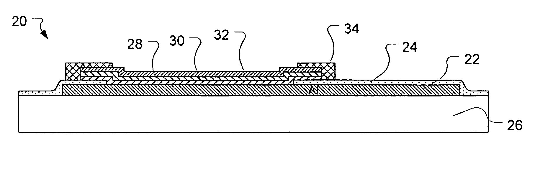
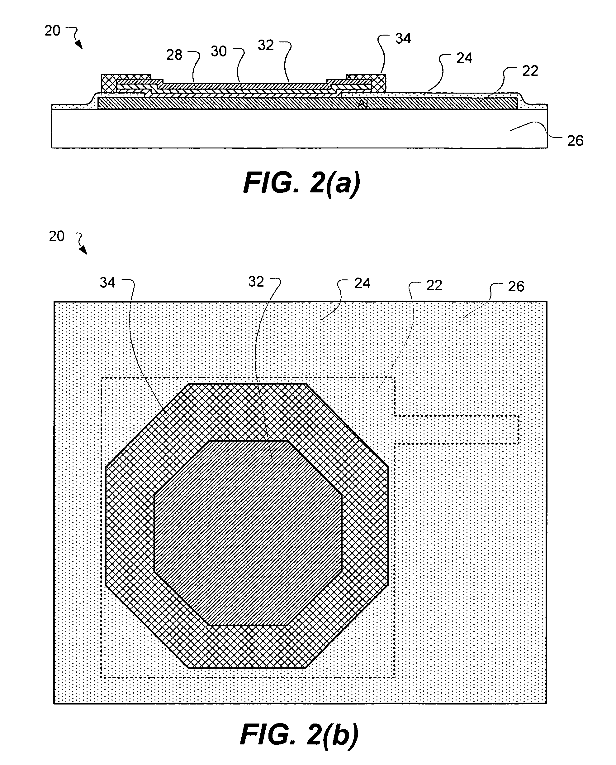
Image

Examples
Embodiment Construction
)
[0017]In describing embodiments of the present invention, the following terminology will be used.
[0018]The singular forms “a,”“an,” and “the” include plural referents unless the context clearly dictates otherwise. Thus, for example, reference to “a layer” includes reference to one or more of such layers, and reference to “an electrical interconnect” includes reference to one or more of such electrical interconnects pads.
[0019]As used herein, the term “about” means that dimensions, sizes, formulations, parameters, shapes and other quantities and characteristics are not and need not be exact, but may be approximated and / or larger or smaller, as desired, reflecting tolerances, conversion factors, rounding off, measurement error and the like and other factors known to those of skill in the art.
[0020]As used herein, the term “adjacent” refers to items which are in close proximity to one another and preferably in direct physical contact with one another.
[0021]As used herein, a plurality ...
PUM
 Abstract
Description
Claims
Application Information
 - R&D
- Intellectual Property
- Life Sciences
- Materials
- Tech Scout
- Unparalleled Data Quality
- Higher Quality Content
- 60% Fewer Hallucinations
Browse by: Latest US Patents, China's latest patents, Technical Efficacy Thesaurus, Application Domain, Technology Topic, Popular Technical Reports.
© 2025 PatSnap. All rights reserved.Legal|Privacy policy|Modern Slavery Act Transparency Statement|Sitemap|About US| Contact US: help@patsnap.com