Dedicated interface architecture for a hybrid integrated circuit

a hybrid integrated circuit and dedicated interface technology, applied in the field of hybrid integrated circuits, can solve the problems of complex design and testing phase of asics, many gates may go unusable, and interfaces run at relatively slow speeds, so as to achieve faster and more efficient communication and less congestion in the system

Inactive Publication Date: 2008-06-17
MICROSEMI SOC
View PDF107 Cites 44 Cited by
  • Summary
  • Abstract
  • Description
  • Claims
  • Application Information

AI Technical Summary

Benefits of technology

[0015]An interface design for a hybrid IC that utilizes dedicated interface tracks to allow signals to interface distributively with the logic blocks of the FPGA portion providing for faster and more efficient communication between the FPGA and ASIC portions of the hybrid IC.
[0016]According to a first embodiment of the present invention, a plurality of dedicated interface tracks are connected directly between the ASIC portion and each individual logic block at the lowest level of the FPGA portion of a hybrid IC. By providing a direct connection from the ASIC portion to individual logic blocks of the FPGA portion, the local routing resources may be bypassed. As a result, there is less congestion in the system.

Problems solved by technology

In an FPGA, however, many of the gates may go unused.
However the design and testing phase of an ASIC is quite complex and expensive because an ASIC must be mask-programmed, and therefore the production of an ASIC only makes fiscal sense when the ASIC is to be produced in large quantities.
First, these interfaces run at relatively slow speeds.
This slow speed is exasperated by the relatively large distances between the logic modules and the interface.
In addition to the routing and speed problems of the prior art interfaces, the fixed pin location and order for signals sent from the ASIC 12 portion to the FPGA 14 portion may cause FPGA place and route difficulties.
Also, the asymmetrical number of I / O connections required for each side of the FPGA portion may also cause FPGA place and route difficulties.
Another drawback of these interfaces is that they require that both the FPGA portion 14 and the ASIC 12 portion be hardwired onto the IC 2 during the design phase.

Method used


Image

  • Dedicated interface architecture for a hybrid integrated circuit
  • Dedicated interface architecture for a hybrid integrated circuit
  • Dedicated interface architecture for a hybrid integrated circuit

Examples


Embodiment Construction

[0032]Those of ordinary skill in the art will realize that the following description of the present invention is illustrative only and not in any way limiting. Other embodiments of the invention will readily suggest themselves to such skilled persons.

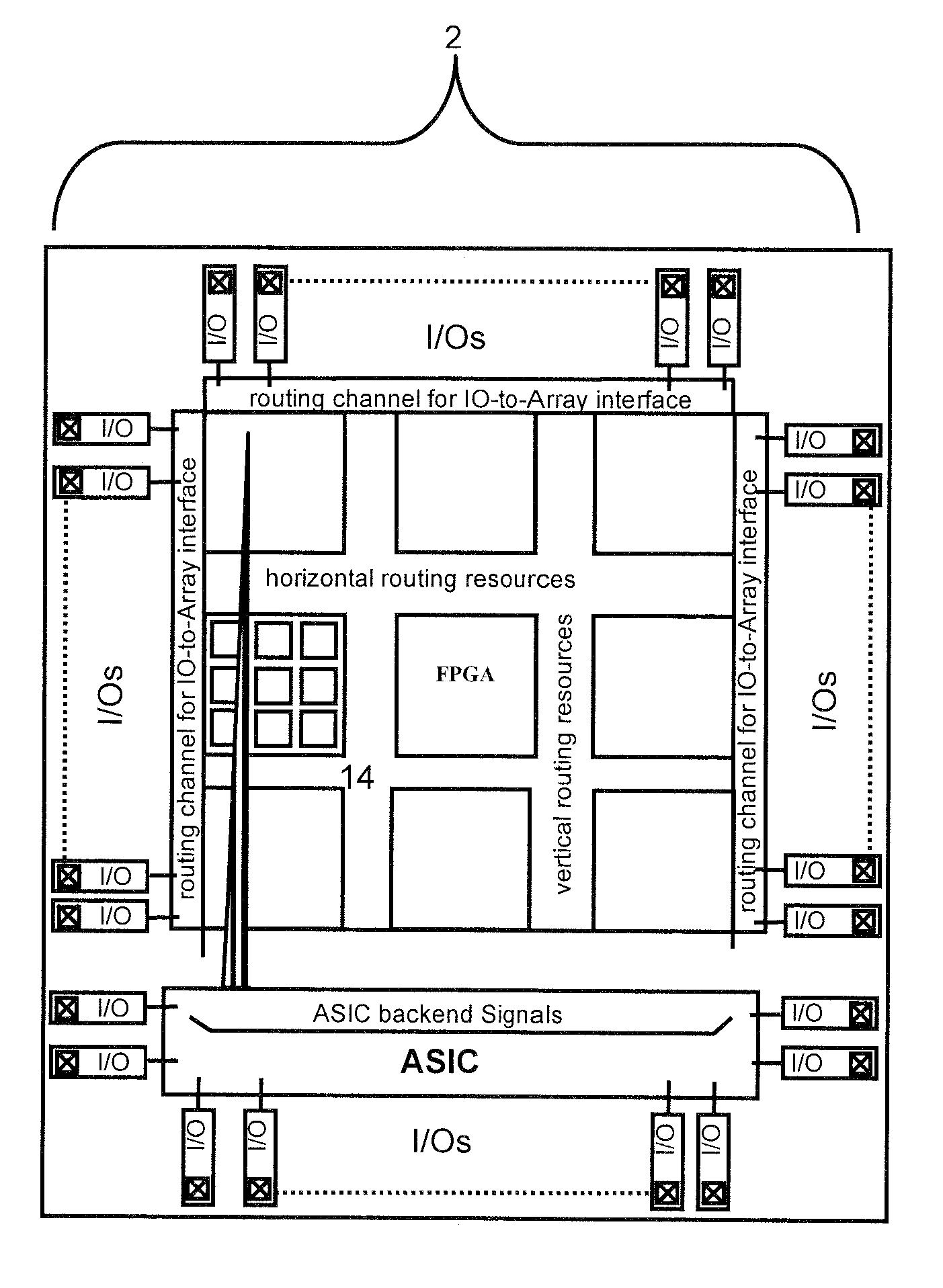
[0033]According to a first embodiment of the present invention, a plurality of dedicated interface tracks are connected directly between the ASIC portion and each individual logic block at the lowest level of the FPGA portion of a hybrid IC. By providing a direct connection from the ASIC portion to individual logic blocks of the FPGA portion, the local routing resources may be bypassed. As a result, there is less congestion in the system.

[0034]According to a second aspect of the present invention, the dedicated interface tracks are connected directly between the ASIC portion to logic blocks at any level of the FPGA portion of a hybrid IC. This design has the advantage of bypassing some of the local routing resources, easing congestion a...


PUM


Abstract

An interface design for a hybrid IC that utilizes dedicated interface tracks to allow signals to interface distributively with the logic blocks of the FPGA portion providing for faster and more efficient communication between the FPGA and ASIC portions of the hybrid IC.

Description

BACKGROUND OF THE INVENTION[0001]1. Field of the Invention[0002]The present invention relates to a hybrid integrated circuit containing an FPGA portion and an ASIC portion. More particularly, this invention relates to an interface between the FPGA and the ASIC portions of a hybrid integrated circuit.[0003]2. The Prior Art[0004]A field programmable gate array (FPGA) may be programmed to execute a wide variety of logic functions, providing designers the ability to design circuits for specific applications. Other advantages of an FPGA are that the design time is short so it can be marketed much quicker and the design is such that can be changed easily. In an FPGA, however, many of the gates may go unused. An application-specific integrated circuit (ASIC), on the other hand, is designed only to perform certain specific tasks, and therefore does not result in wasted gates. However the design and testing phase of an ASIC is quite complex and expensive because an ASIC must be mask-programm...

Claims


Application Information

Patent Timeline
Patent Type & Authority Patents(United States)
IPC IPC(8): G06F17/50H03K19/177
CPCG06F15/7867H03K19/177
Inventor CHAN, KING W.SHU, WILLIAM C. T.KAPTANOGLU, SINANCHENG, CHI FUNG
Owner MICROSEMI SOC
Why Eureka
Try Eureka