High-frequency switch

a high-frequency switch and switch technology, applied in the field of high-frequency switches, can solve the problems of increased design load, increased cost, and faulty operation of radar or communication devices

Active Publication Date: 2008-08-12
MITSUBISHI ELECTRIC CORP
View PDF7 Cites 23 Cited by
  • Summary
  • Abstract
  • Description
  • Claims
  • Application Information

AI Technical Summary

Benefits of technology

[0016]The present invention has been made to solve the above problems. It is a first object of the present invention to configure a high-frequency switch so that the characteristic impedance of a connection end on the switch-OFF side is close to the characteristic impedance of a high-frequency transmission system. As a result, the resonance within the package is inhibited at the time of switching so that a low-cost, high-reliability, high-frequency switch can be offered.
[0018]Accordingly, in the high-frequency switch according to the present invention, the matching semiconductor element is ON as the switching element in the branch path on the switch-OFF side is ON. Thus, the ON resistor for the matching semiconductor element is coupled between the grounding end and the stub of the matching circuit. The ON resistor achieves matching with ease so that the characteristic impedance at the connection end on the switch-OFF side is close to the characteristic impedance of the high-frequency transmission system connected to the connection end. Therefore, the reflection loss at the connection end on the switch-OFF side can be reduced. This also makes it possible to inhibit intra-package resonance, which is likely to occur at the time of switching.

Problems solved by technology

If resonance occurs within the package, the operations of a radar or communication apparatus may become faulty.
It means that an extra design load increases.
It means that the cost increases due to a change in the package size.

Method used


Image

  • High-frequency switch
  • High-frequency switch
  • High-frequency switch

Examples


first embodiment

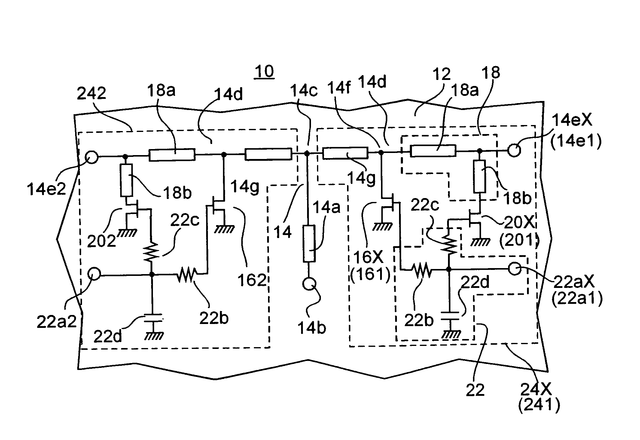
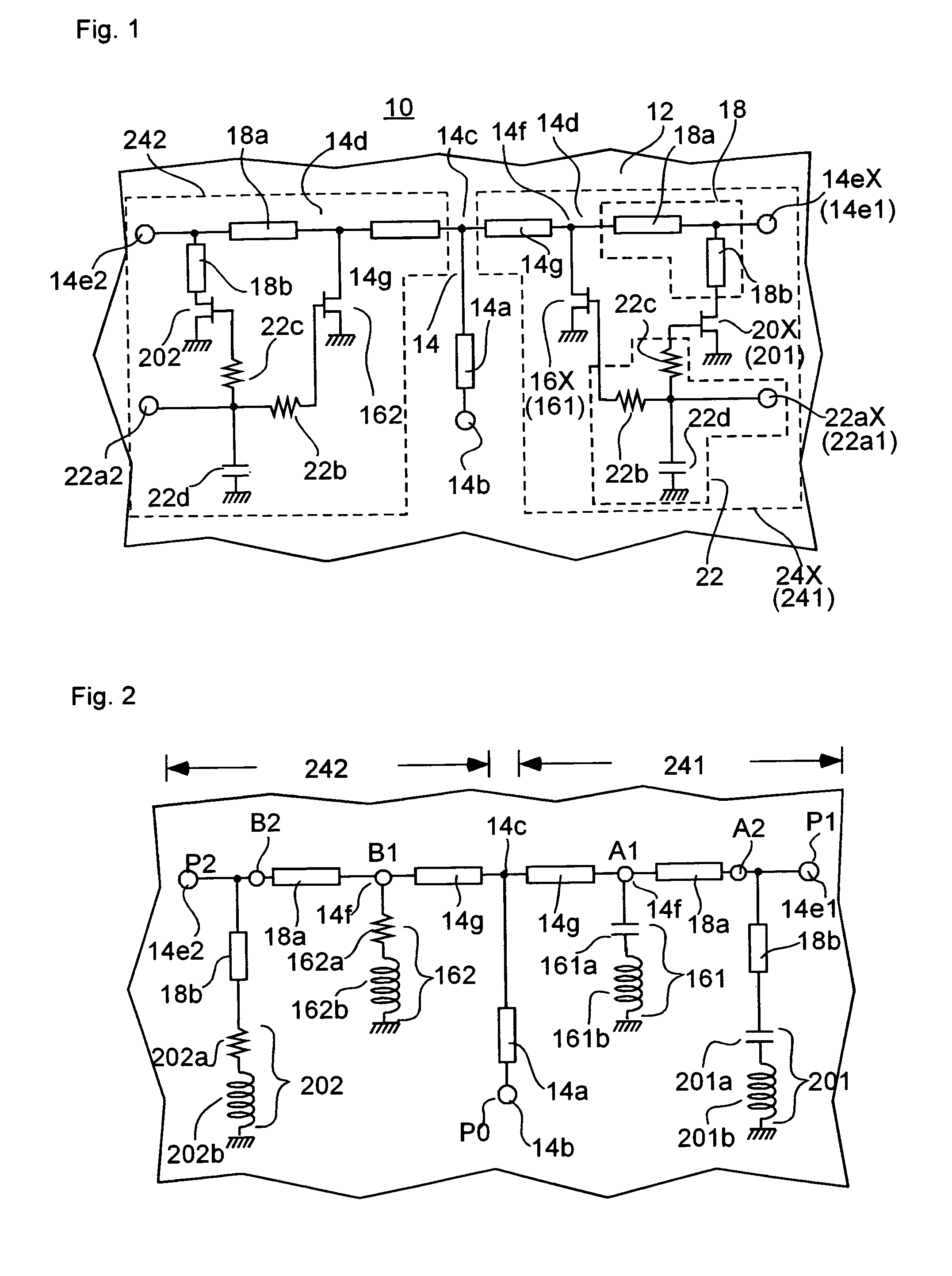
[0034]FIG. 1 is a circuit diagram illustrating a high-frequency switch according to an embodiment of the present invention.

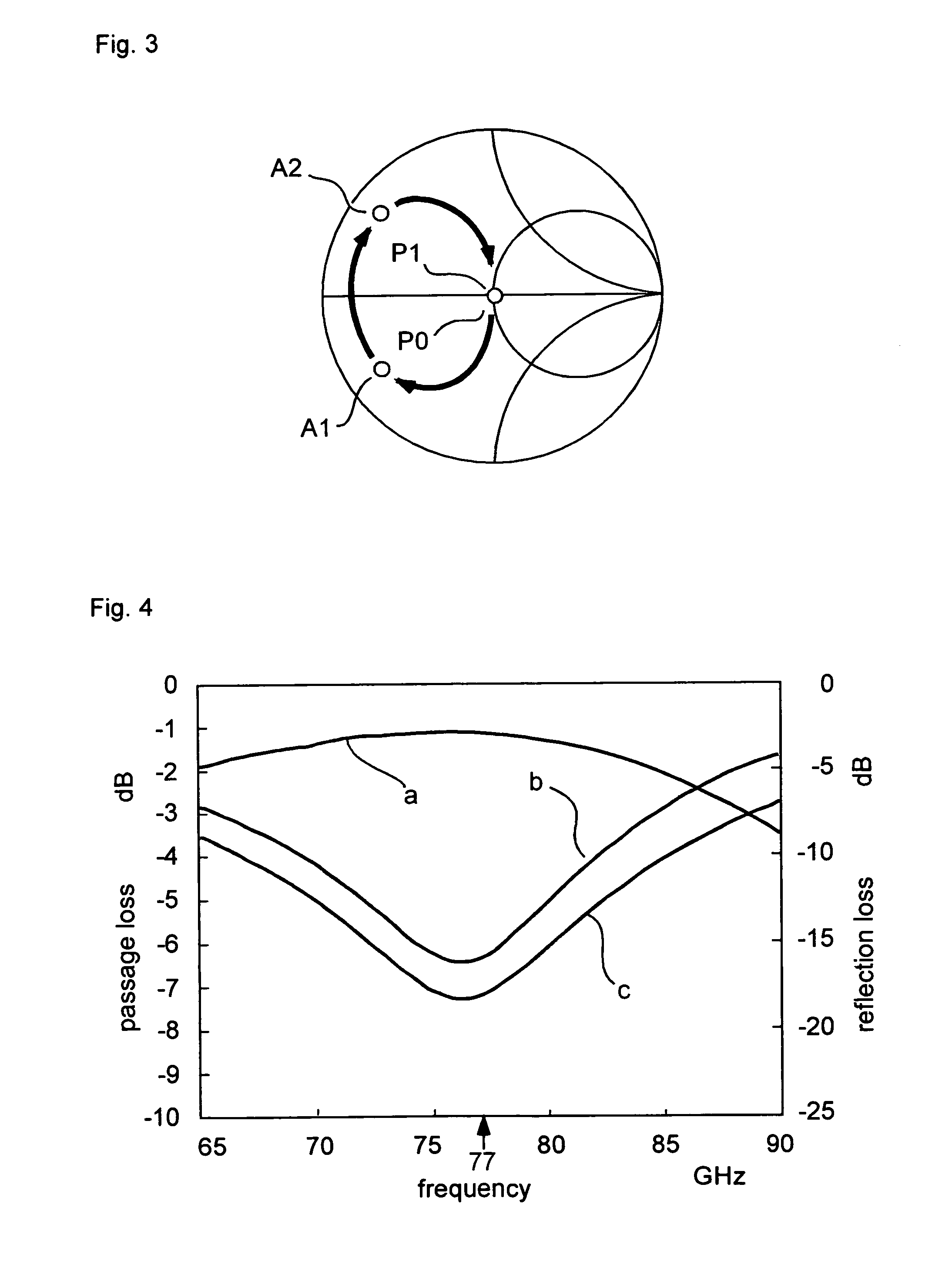
[0035]The high-frequency switch 10, which is shown in FIG. 1, is a two-branch switch operating in, for instance, a 77 GHz band, that is, an SPDT switch. Two unit switches 24X (X=1 or 2) are positioned after a branch point 14c in an input connection path 14a, which is a common path. Each unit switch 24X comprises a signal path 14, which includes a λ / 4 transmission path 14g, an FET 16X (X=1 or 2), an output matching circuit 18, a matching FET 20X (X=1 or 2), and a control circuit 22. Further, various circuit elements are positioned on a GaAs substrate 12 serving as a substrate.

[0036]The variable X, which is attached to circuit element reference numerals for the unit switches 24X, varies with the variable X of a unit switch. If, for instance, the reference numeral of a specific unit switch shown in a figure is 241 (that is, when X=1 at 24X), the output end 14eX, wh...

first modified embodiment

[0071]The configuration of a high-frequency switch according to a first modified embodiment is basically the same as that of the high-frequency switch 10 according to the first embodiment. In the high-frequency switch according to the first modified embodiment, the semiconductor element which is used as switching element and matching semiconductor element are connected to separate control input ends. The control voltage for the matching semiconductor element is separated from the semiconductor element, which is used as a switching element. The control voltage can be applied as desired so that the ON voltage of the matching semiconductor element is adjustable.

[0072]FIG. 7 is a circuit diagram illustrating the first modified embodiment of a high-frequency switch according to one embodiment of the present invention.

[0073]In FIG. 7, the high-frequency switch 30 has the same basic configuration as the high-frequency switch 10 according to the first embodiment. However, the first modified...

second modified embodiment

[0083]The high-frequency switch according to a second modified embodiment has basically the same configuration as the high-frequency switch 30 according to the first modified embodiment. However, the high-frequency according to the second modified embodiment uses diodes as the switching element and matching semiconductor element instead of FETs. The other circuit configuration changes are made due to the use of such diodes.

[0084]FIG. 9 is a circuit diagram illustrating a high-frequency switch according to one modified embodiment of the present invention.

[0085]As indicated in FIG. 9, the high-frequency switch 35 according to the second modified embodiment differs in configuration from the high-frequency switch 30 according to the first modified embodiment in that a direct-current-interrupting capacitor 38 is positioned between the branch point 14c and λ / 4 transmission path 14g. A diode 40X (X=1 or 2) is used in place of the FET 16X. A shunt connection is established between the branc...


PUM


Abstract

A high-frequency switch operating in a millimeter wave band that includes a signal path having a λ / 4 transmission path, for part of two or more branch signal paths that branch from an input connection path via a branch point; an FET, which is shunt-connected between a grounding end and the branch signal paths that are positioned between the λ / 4 transmission path and a terminal end, as viewed from the branch point, and used to connect or disconnect the branch signal paths and the grounding end; an output matching circuit, which is positioned on the branch signal paths that are positioned between a terminal end and a connection point for the FET as viewed from the branch point, and includes a shunt-connected stub; and a matching FET, which is connected between the stub and the grounding end and used to connect or disconnect the stub and the grounding end in accordance with the FET's connection / disconnection.

Description

BACKGROUND OF THE INVENTION[0001]1. Field of the Invention[0002]The present invention relates to a high-frequency switch, and more particularly to a high-frequency switch that is used to provide RF signal switching for radars and communication apparatuses operating in a millimeter wave band.[0003]2. Description of the Related Art[0004]The application of a microwave device increasingly progresses in accordance with an increase in the degree of computerization. Microwave devices are applied to various fields. For example, there are microwave devices for use in cellular phones, which use a relatively low frequency, microwave devices for use in high-frequency telecommunication, and microwave devices for use in telecommunication equipment such as high-frequency vehicle-mounted radars and observation satellites.[0005]Recently, a small-size, high-speed, high-frequency switch based on a microwave IC (MIC) was developed as a high-speed switch. Further, an MMIC (Monolithic Microwave IC), whic...

Claims


Application Information

Patent Timeline
Patent Type & Authority Patents(United States)
IPC IPC(8): H01P1/10H01P5/12
CPCH01P1/15H03H11/28
Inventor TSUKAHARA, YOSHIHIRO
Owner MITSUBISHI ELECTRIC CORP
Why Eureka
Try Eureka