Semiconductor memory device having a redundancy information memory directly connected to a redundancy control circuit

a technology of memory device and redundancy control circuit, which is applied in the direction of static storage, digital storage, instruments, etc., can solve the problems of slowing down the access to memory cells and poor performance, and achieve the effect of improving the access performance of semiconductor memory devices and reducing the chip area required for the redundancy system

Inactive Publication Date: 2008-08-12
POLARIS INNOVATIONS LTD
View PDF7 Cites 63 Cited by
  • Summary
  • Abstract
  • Description
  • Claims
  • Application Information

AI Technical Summary

Benefits of technology

[0008]Therefore, in one aspect, the present invention provides an improved semiconductor memory device in which the chip area required for the redundancy system is reduced and the access performance of the semiconductor memory device is improved. In a further aspect, the invention provides a method for operating such a semiconductor memory device.

Problems solved by technology

For these steps, a total number of about twenty clock cycles is necessary, which slows down the access to the memory cells and leads to poor performance.

Method used


Image

  • Semiconductor memory device having a redundancy information memory directly connected to a redundancy control circuit
  • Semiconductor memory device having a redundancy information memory directly connected to a redundancy control circuit
  • Semiconductor memory device having a redundancy information memory directly connected to a redundancy control circuit

Examples


Embodiment Construction

[0027]The making and using of the presently preferred embodiments are discussed in detail below. It should be appreciated, however, that the present invention provides many applicable inventive concepts that can be embodied in a wide variety of specific contexts. The specific embodiments discussed are merely illustrative of specific ways to make and use the invention, and do not limit the scope of the invention.

[0028]An embodiment of the present invention will be described in detail below with reference to the accompanying drawings.

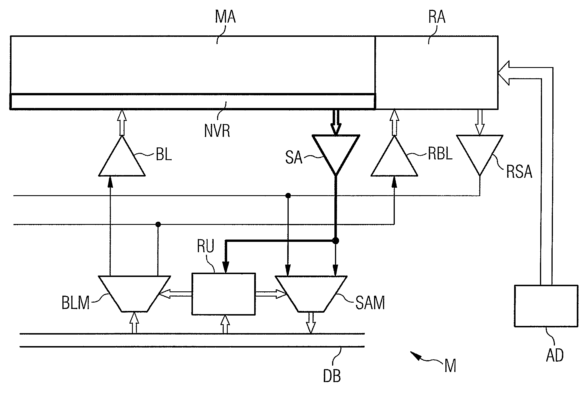
[0029]FIG. 3 illustrates an embodiment according to the invention. The semiconductor memory device M comprises a memory array MA, a redundancy array RA, and a non-volatile redundancy information memory NVR. The three memories may be separate and implemented in different memory technologies. However, it is advantageous if they are of the same memory type as they can be manufactured and integrated together and share the same I / O peripherals.

[0030]By connect...


PUM


Abstract

A semiconductor memory device (M) includes a memory array (MA) having a plurality of memory cells, a redundancy array (RA) having a plurality of memory cells, a non-volatile redundancy information memory (NVR) having a plurality of memory cells for storing redundancy information, and a redundancy control unit (RU) for selecting either memory cells in the memory array (MA) or memory cells in the redundancy array (RA). In one example, the non-volatile redundancy information memory (NVR) is connected directly to the redundancy control unit (RU) by means of at least one sense amplifier (SA).

Description

TECHNICAL FIELD[0001]The present invention relates to a semiconductor memory device and also concerns a method for operating such a semiconductor memory device.BACKGROUND[0002]As the storage capacity of semiconductor memory devices continues to increase, the number of memory cells included in such memories also increases. With the increase in the number of memory cells, the probability that one or more memory cells are defective is increased. In order to avoid having to discard the memory device due to just one or a few defective memory cells, redundant memory elements are included in the semiconductor memory device. The redundant memory elements are usually rows and / or columns and are used to replace the rows and / or columns that contain defective memory cells.[0003]During wafer testing, all memory cells are tested. The information about which memory cells are defective and sometimes the information about which redundant memory elements are selected to replace the defective memory e...

Claims


Application Information

Patent Timeline
Patent Type & Authority Patents(United States)
IPC IPC(8): G11C29/44
CPCG11C29/846G11C29/789
Inventor NITZAN, IFATBEN-ARI, NIMROD
Owner POLARIS INNOVATIONS LTD
Why Eureka
Try Eureka