

Semiconductor device and method for producing the same
a technology of semiconductor devices and power supply connections, which is applied in the direction of semiconductor/solid-state device testing/measurement, semiconductor/solid-state device details, instruments, etc., can solve the problems of wlbi cannot be employed in this device, voltage application cannot be achieved in all separate power supplies, and the number of electrically-connectable and probeable pads over one wafer is limited, so as to reduce the number of terminals.
- Summary
- Abstract
- Description
- Claims
- Application Information
AI Technical Summary
Benefits of technology
Problems solved by technology
Method used
Image

Examples
embodiment 1
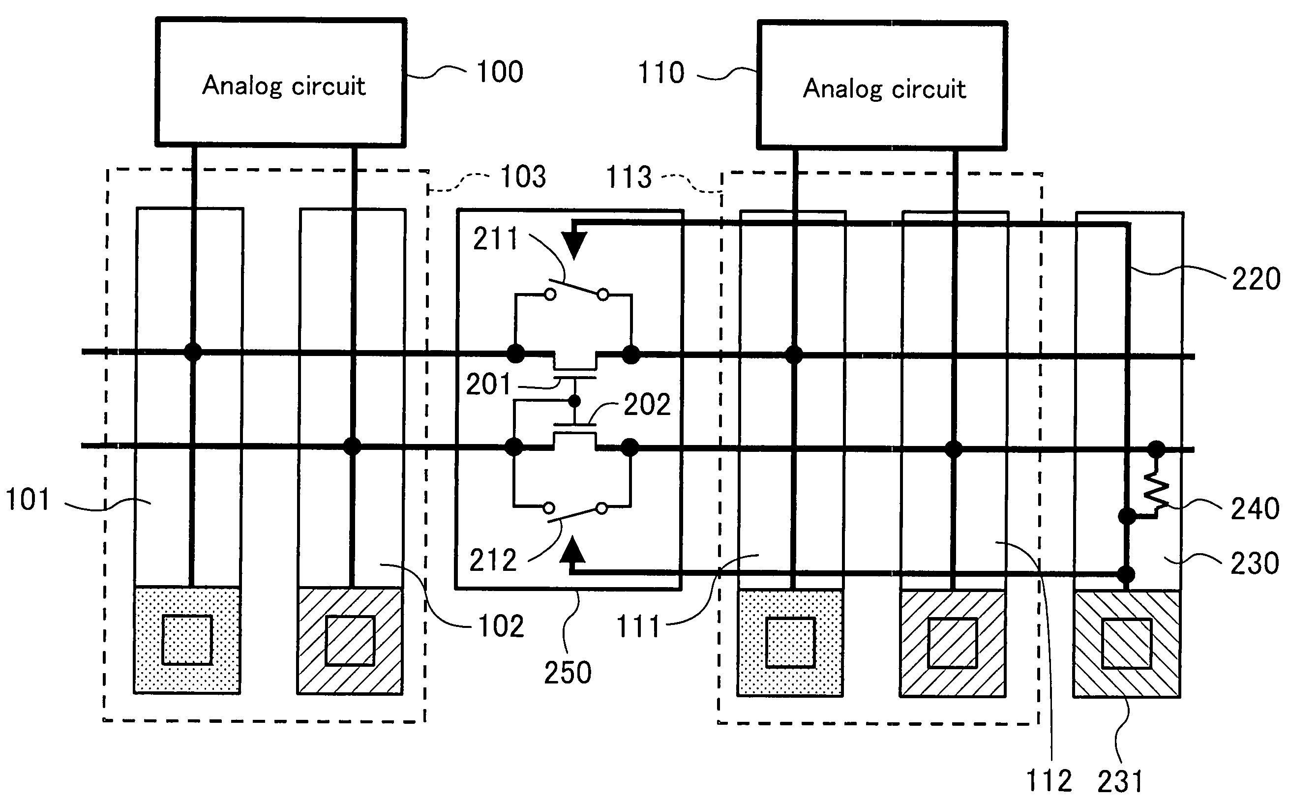
[0036]FIG. 1 is a circuit diagram showing a semiconductor device according to embodiment 1 of the present invention. In FIG. 1, reference numerals 100 and 110 denote analog circuits having predetermined functions, each of which requires a separate power supply in order to avoid effects of noise, and the like. Reference numeral 103 denotes an analog IO region for the analog circuit 100, which includes a VDD terminal 101 for supplying an externally-input VDD voltage to the analog circuit 100 and a VSS terminal 102 for supplying an externally-input VSS voltage to the analog circuit 100. Reference numeral 113 denotes an analog IO region for the analog circuit 110, which includes a VDD terminal 111 for supplying an externally-input VDD voltage to the analog circuit 110 and a VSS terminal 112 for supplying an externally-input VSS voltage to the analog circuit 110. The IO regions 103 and 113 each have two power supply cells. Each power supply cell includes a protection circuit, a VDD or VS...
embodiment 2
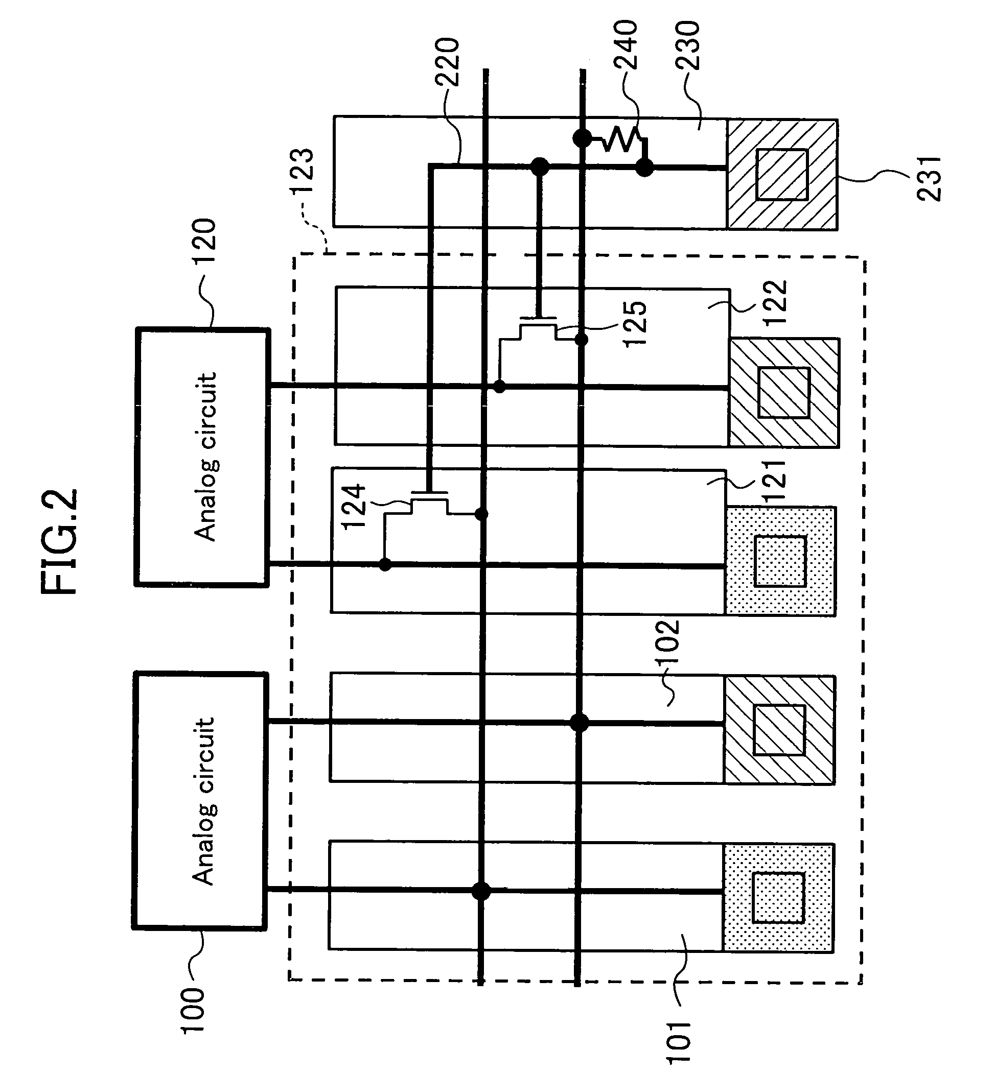
[0050]FIG. 2 is a circuit diagram showing a semiconductor device according to embodiment 2 of the present invention. It should be noted that like elements are denoted by like reference numerals used in FIG. 1, and therefore, descriptions thereof are herein omitted.
[0051]In embodiment 2, a VDD terminal 101 and a VSS terminal 102 which supply a supply voltage to an analog circuit 100 and a VDD terminal 121 and a VSS terminal 122 which supply a supply voltage to an analog circuit 120 are placed in the same analog IO region 123. The analog IO region 123 includes protection transistors 124 and 125 between power supplies as connection means.
[0052]The semiconductor device of embodiment 2 does not include the power supply disconnection cell 250 which has been described in embodiment 1. One of the source and drain of the protection transistor 124 is connected to the VDD terminal 101, and the other one is connected to the VDD terminal 121. The protection transistor 124 controls disconnection ...
PUM
 Abstract
Description
Claims
Application Information