
Semiconductor device and method for producing the same

a technology of semiconductor devices and power supply connections, which is applied in the direction of semiconductor/solid-state device testing/measurement, semiconductor/solid-state device details, instruments, etc., can solve the problems of wlbi cannot be employed in this device, voltage application cannot be achieved in all separate power supplies, and the number of electrically-connectable and probeable pads over one wafer is limited, so as to reduce the number of terminals.

Inactive Publication Date: 2005-03-31
PANASONIC CORP
View PDF1 Cites 7 Cited by
  • Summary
  • Abstract
  • Description
  • Claims
  • Application Information

AI Technical Summary

Benefits of technology

"The present invention provides a semiconductor device that achieves effective WLBI (voltage application to all power supply pads without reducing input / output signals) with a control signal, while also protecting power supply cells from surge breakdown. The semiconductor device includes a plurality of circuits, power supply cells, and a protection transistor for controlling electrical connection among the power supply cells. The protection transistor is controlled based on a difference in voltage between input terminals of the power supply cells. The semiconductor device also includes a disconnectable line connected in parallel to the protection transistor for further protection. The invention provides a semiconductor device production method that includes forming the semiconductor device, inspecting it, and disconnecting the disconnectable line. The technical effects of the present invention include achieving effective WLBI with a control signal, protecting power supply cells from surge breakdown, and reducing the size of the semiconductor device."

Problems solved by technology

However, the number of electrically-connectable and probeable pads over one wafer is limited due to the flatness of the wafer, the probe pressure against the wafer, and the like.
As a result, voltage application cannot be achieved in all of the separate power supplies in an LSI device of a multi power supply design, and WLBI cannot be employed in this device.
However, this results in an increase in the chip area and causes an increase in cost.
Furthermore, since short-circuited transistors do not function as protection transistors, deterioration in quality may be caused due to a surge, or the like.

Method used


Image

  • Semiconductor device and method for producing the same
  • Semiconductor device and method for producing the same
  • Semiconductor device and method for producing the same

Examples


embodiment 1

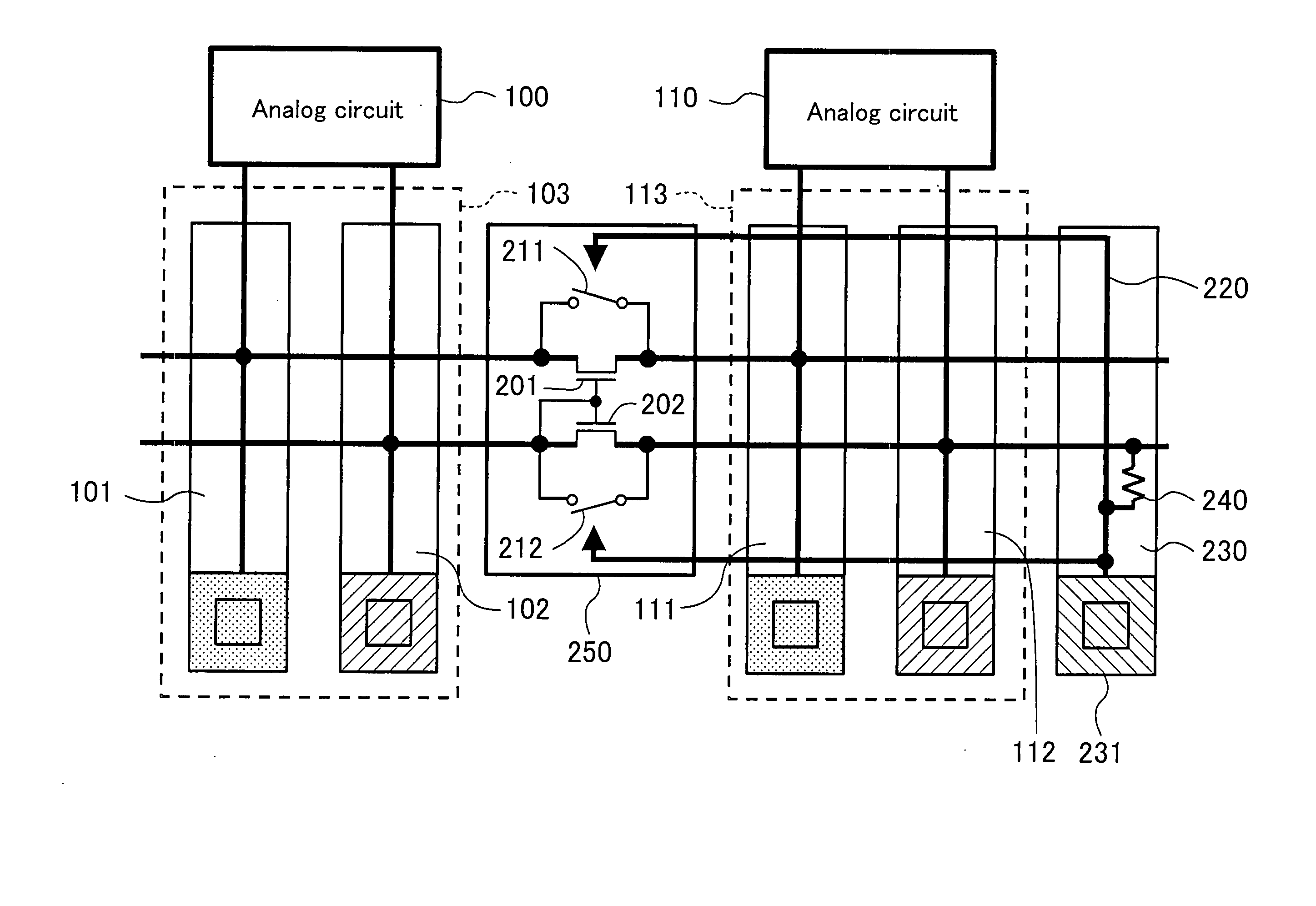
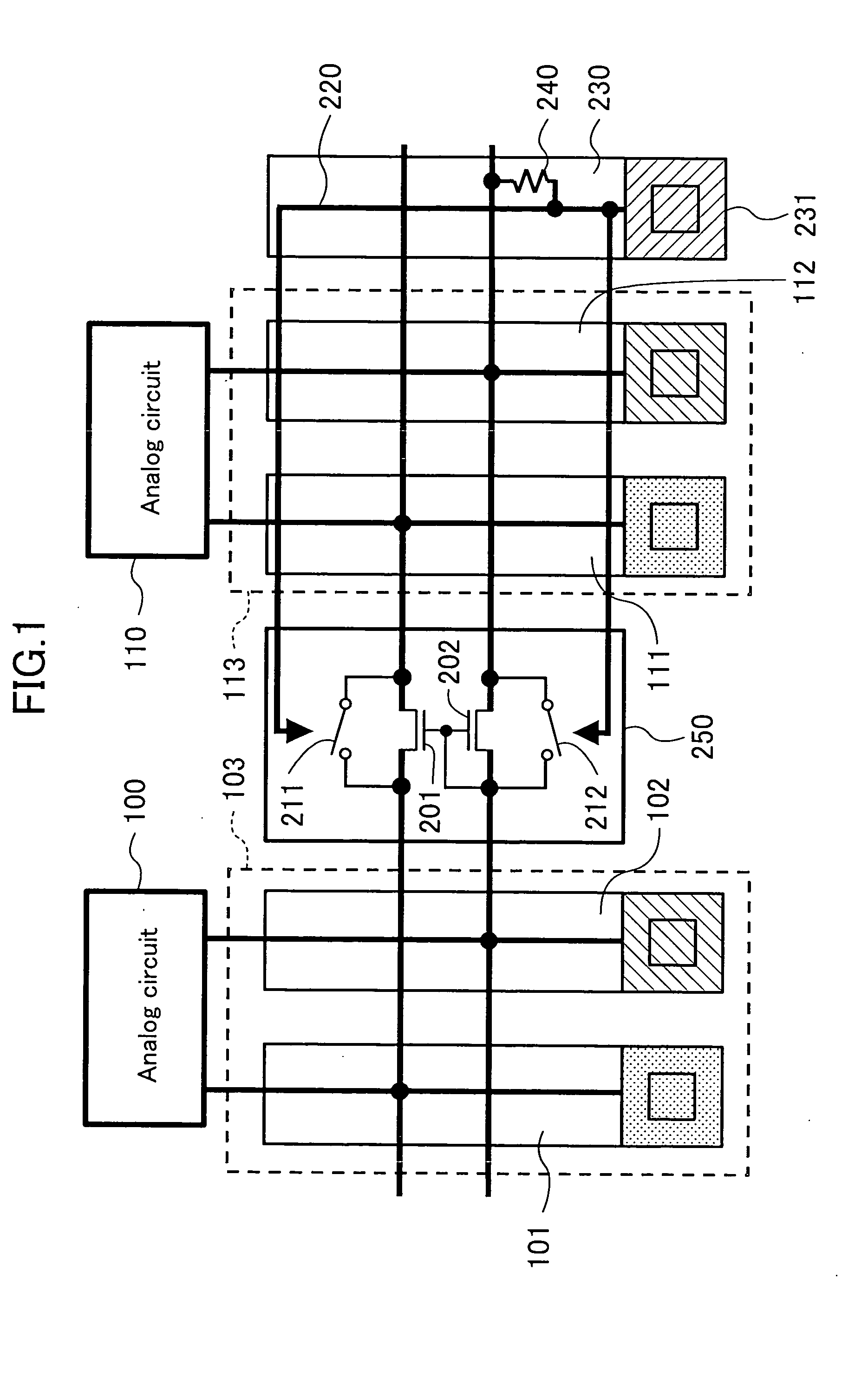
[0036]FIG. 1 is a circuit diagram showing a semiconductor device according to embodiment 1 of the present invention. In FIG. 1, reference numerals 100 and 110 denote analog circuits having predetermined functions, each of which requires a separate power supply in order to avoid effects of noise, and the like. Reference numeral 103 denotes an analog IO region for the analog circuit 100, which includes a VDD terminal 101 for supplying an externally-input VDD voltage to the analog circuit 100 and a VSS terminal 102 for supplying an externally-input VSS voltage to the analog circuit 100. Reference numeral 113 denotes an analog IO region for the analog circuit 110, which includes a VDD terminal 111 for supplying an externally-input VDD voltage to the analog circuit 110 and a VSS terminal 112 for supplying an externally-input VSS voltage to the analog circuit 110. The IO regions 103 and 113 each have two power supply cells. Each power supply cell includes a protection circuit, a VDD or VS...

embodiment 2

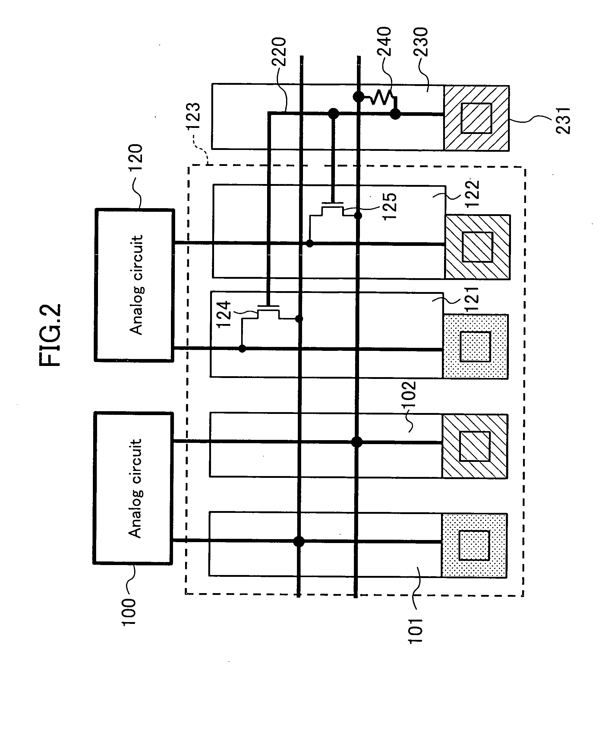
[0050]FIG. 2 is a circuit diagram showing a semiconductor device according to embodiment 2 of the present invention. It should be noted that like elements are denoted by like reference numerals used in FIG. 1, and therefore, descriptions thereof are herein omitted.

[0051] In embodiment 2, a VDD terminal 101 and a VSS terminal 102 which supply a supply voltage to an analog circuit 100 and a VDD terminal 121 and a VSS terminal 122 which supply a supply voltage to an analog circuit 120 are placed in the same analog IO region 123. The analog IO region 123 includes protection transistors 124 and 125 between power supplies as connection means.

[0052] The semiconductor device of embodiment 2 does not include the power supply disconnection cell 250 which has been described in embodiment 1. One of the source and drain of the protection transistor 124 is connected to the VDD terminal 101, and the other one is connected to the VDD terminal 121. The protection transistor 124 controls disconnect...


PUM


Abstract

In a power supply disconnection cell, a power supply connection switch is added in parallel to a protection transistor having a fixed gate. The power supply connection switch electrically connects or disconnects a plurality of power supplies according to a control signal externally input through an external control terminal. In a WLBI process, a plurality of power supplies are connected by the power supply connection switch, and therefore, a voltage is applied to other power supply pads by voltage application to a specific input terminal. After the WLBI process, the power supplies are disconnected, and electric charges produced by an abnormal voltage, such as a surge, or the like, are released by the protection transistor provided between the power supplies, whereby breakdown of a semiconductor device is prevented.

Description

BACKGROUND OF THE INVENTION [0001] The present invention relates to a power supply disconnection system for a semiconductor device, which has the function of controlling connection and disconnection between a plurality of power supplies in the semiconductor device and the function of preventing a surge breakdown after a package assembling process, such that the number of power supplies which apply a voltage in a wafer level burn-in (WLBI) process can be reduced. [0002] In recent years, along with the advancement of functional synthesis in a system LSI device, a larger number of system LSI devices have incorporated analog circuits. Further, a separate power supply which is disconnected from the other power supplies is necessary for each analog circuit in order to avoid effects of noise, and the like. To this end, multi power supply design in LSI devices has been becoming mainstream. [0003] In addition, a process technique whose resolution has been increasing is employed, and accordin...

Claims


Application Information

Patent Timeline
Patent Type & Authority Applications(United States)
IPC IPC(8): G01R31/30G01R31/28G11C29/00H01L21/66H01L21/82H01L21/822H01L23/528H01L27/02H01L27/04H02J1/00
CPCH01L23/5286H01L27/0203H01L27/0251H01L2924/0002H01L2924/00
Inventor KAWANISHI, KEISHIMAZU, NORIYUKIMORITA, AYAKO
Owner PANASONIC CORP
Learn More