Image sensor

a technology of image sensor and addressing circuit, which is applied in the field of image sensor, can solve the problems of image sensor requiring a slightly more complex addressing circuit, reducing the surface area of the pixels, and reducing the sensitivity of the image sensor, so as to achieve good sensitivity, good quality, and reliable with time.

Inactive Publication Date: 2008-08-26
STMICROELECTRONICS SRL
View PDF3 Cites 39 Cited by
  • Summary
  • Abstract
  • Description
  • Claims
  • Application Information

AI Technical Summary

Benefits of technology

[0016]An object of the present invention is to provide an image sensor having “compact” pixels exhibiting a very good sensitivity, enabling performing light intensity measurements of good quality, which are reliable with time.
[0017]Another object of the present invention is to provide such an image sensor of simple structure.

Problems solved by technology

However, when the pixel size is desired to be decreased to increase the number of pixels on a given surface, the sizes of access transistor 2 and of transistors T1 to T3 cannot be sufficiently decreased, to keep a sufficient variation range of the voltage at node n, and the surface area decrease of the pixels is performed to the detriment of the surface taken up by the photodiode.
This results in significantly decreasing the sensitivity of the image sensor pixels.
However, such an image sensor requires a slightly more complex addressing circuit.
This provides a gain in surface area but this gain remains insufficient for the smallest pixels.
However, the measurements performed by such pixels contain much more noise than those performed by 4-transistor pixels.
Since a sampling of the precharge voltage of node n cannot be performed prior to the progressive discharge of node n according to the captured photons, the differential reading does not enable suppressing this kTC noise, conversely to the reading of a 4-transistor type pixel.
However, in addition to the above-mentioned disadvantages relative to 3-transistor pixels, the forming of PIN-type photodiodes in amorphous silicon has many disadvantages, and especially a premature aging of layer 46 in the presence of intense light.

Method used


Image

  • Image sensor
  • Image sensor
  • Image sensor

Examples


Embodiment Construction

[0035]For clarity, the same elements have been designated with the same reference numerals in the different drawings and, further, as usual in the representation of integrated circuits, FIGS. 1, 3, 4, and 5 are not drawn to scale.

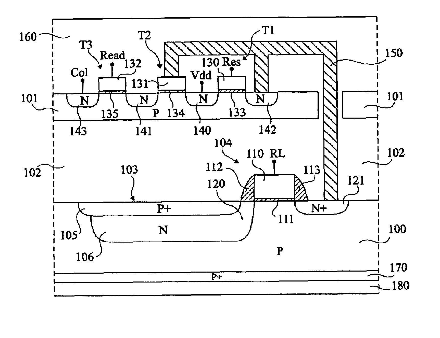
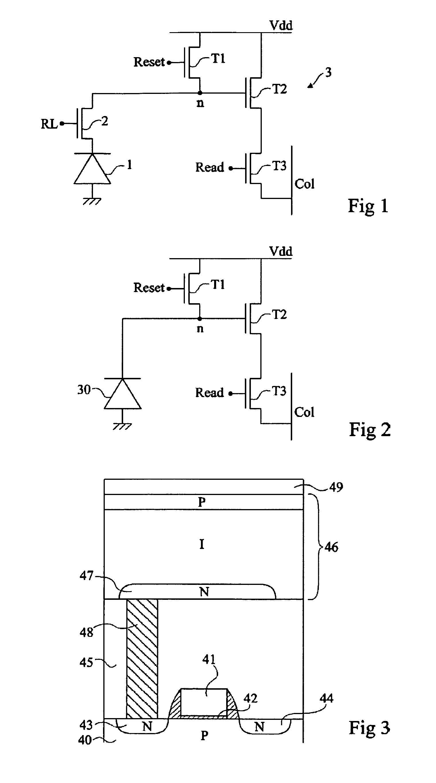
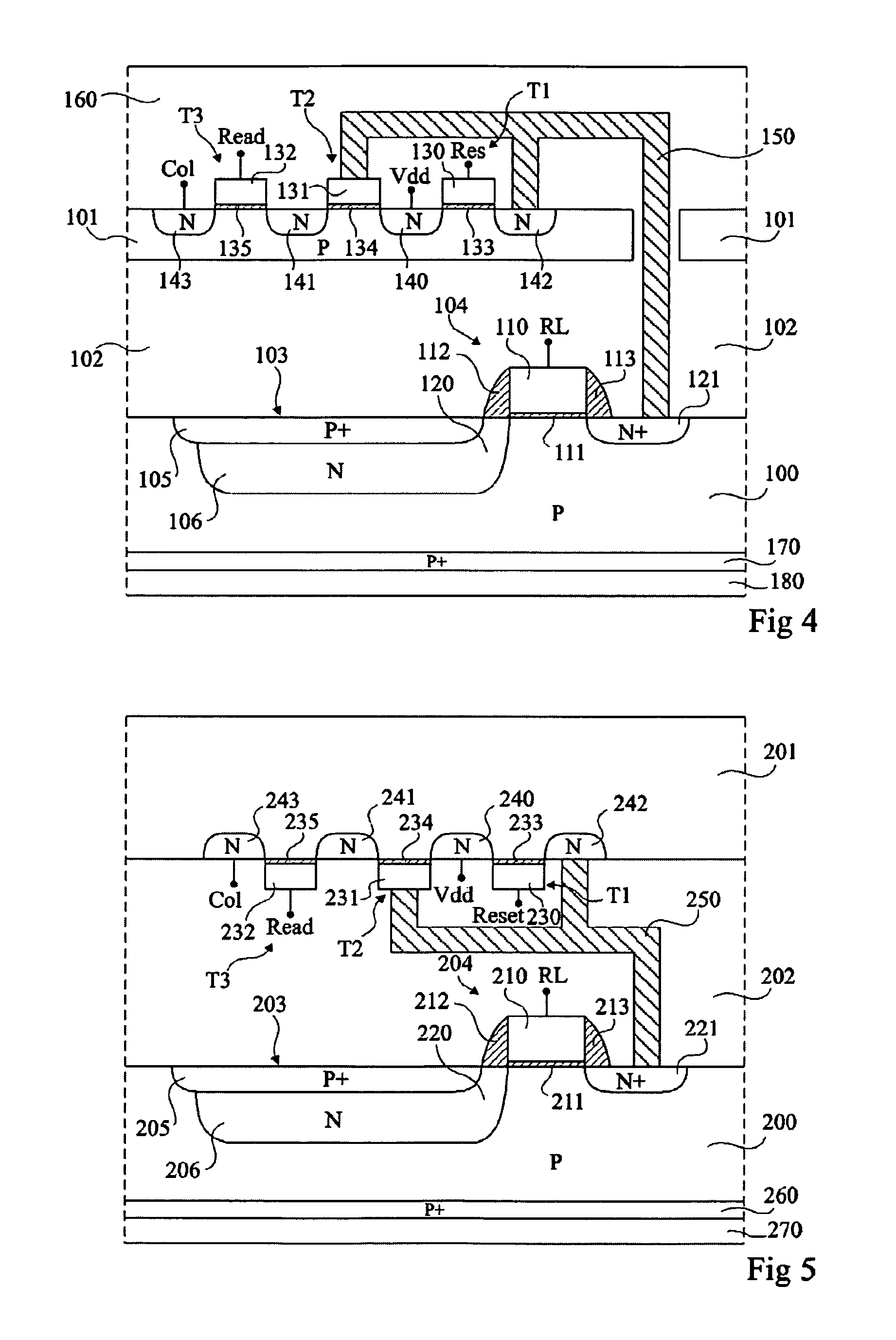
[0036]An image sensor according to the present invention comprises pixels of 4-transistor type, such as described in FIG. 1. The photodiodes and the access transistors of the pixels are formed in a “lower” semiconductor substrate, and the transistors of the read circuit are formed in an “upper” semiconductor substrate. The two substrates are superposed and separated from each other by an insulating layer. The read transistors are thus placed above the photodiodes and the access transistors. Further, the photodiodes receive incident transistors arriving on the lower surface side of the lower substrate, opposite to the insulating layer and to the upper substrate.

[0037]Examples of embodiment of an image sensor according to the present invention are described i...


PUM


Abstract

An image sensor including a pixel assembly, each pixel including a photodiode and an access transistor connected to a read circuit, the photodiode and the access transistor being formed in and above a first semiconductor substrate, all or part of the read circuit being formed in a second semiconductor substrate, the second substrate being placed above the first substrate and separated therefrom by an intermediary insulating layer covering the access transistor, the photodiode receiving incident photons on its lower surface side opposite to the intermediary insulating layer.

Description

BACKGROUND OF THE INVENTION[0001]1. Field of the Invention[0002]The present invention relates to an image sensor formed of a pixel assembly, each pixel comprising a photodiode.[0003]2. Discussion of the Related Art[0004]FIG. 1 is a diagram of a pixel of an image sensor of “4 transistors” type. The pixel comprises a photodiode 1, an access transistor 2, and a read circuit 3. The anode of the photodiode is grounded. The cathode of photodiode 1 is connected to a row line RL. The drain of access transistor 2 is connected to the source of access transistor 2. The gate of access transistor 2 is connected to a node n. Read circuit 3 is formed of three N-channel MOS transistors T1, T2, T3. The source of transistor T1 and the gate of transistor T2 are connected to node n. The drains of transistors T1 and T2 are connected to a supply voltage Vdd. Transistor T1 is controlled by a reset signal Reset. The source of transistor T2 is connected to the drain of transistor T3 which is controlled by a...

Claims


Application Information

Patent Timeline
Patent Type & Authority Patents(United States)
IPC IPC(8): H01L27/148
CPCH01L27/14609H01L27/14634H01L27/14603H01L27/1469H01L27/14636H01L27/14643
Inventor CAZAUX, YVONHERAULT, DIDIER
Owner STMICROELECTRONICS SRL
Why Eureka
Try Eureka