Supercharge Your Innovation With Domain-Expert AI Agents!

Current source cell arrangement and digital-to-analog converter

a current source cell and converter technology, applied in the direction of digital-analog converters, transmission systems, instruments, etc., can solve the problems of differential linearity error or non-linearity (integral linearity) error, difficult implementation, and inability to maintain constant output current value of each current source cell, etc., to achieve the effect of extending the applicability of the arrangement structur

Inactive Publication Date: 2008-09-02
RENESAS ELECTRONICS CORP
View PDF6 Cites 1 Cited by
  • Summary
  • Abstract
  • Description
  • Claims
  • Application Information

AI Technical Summary

Benefits of technology

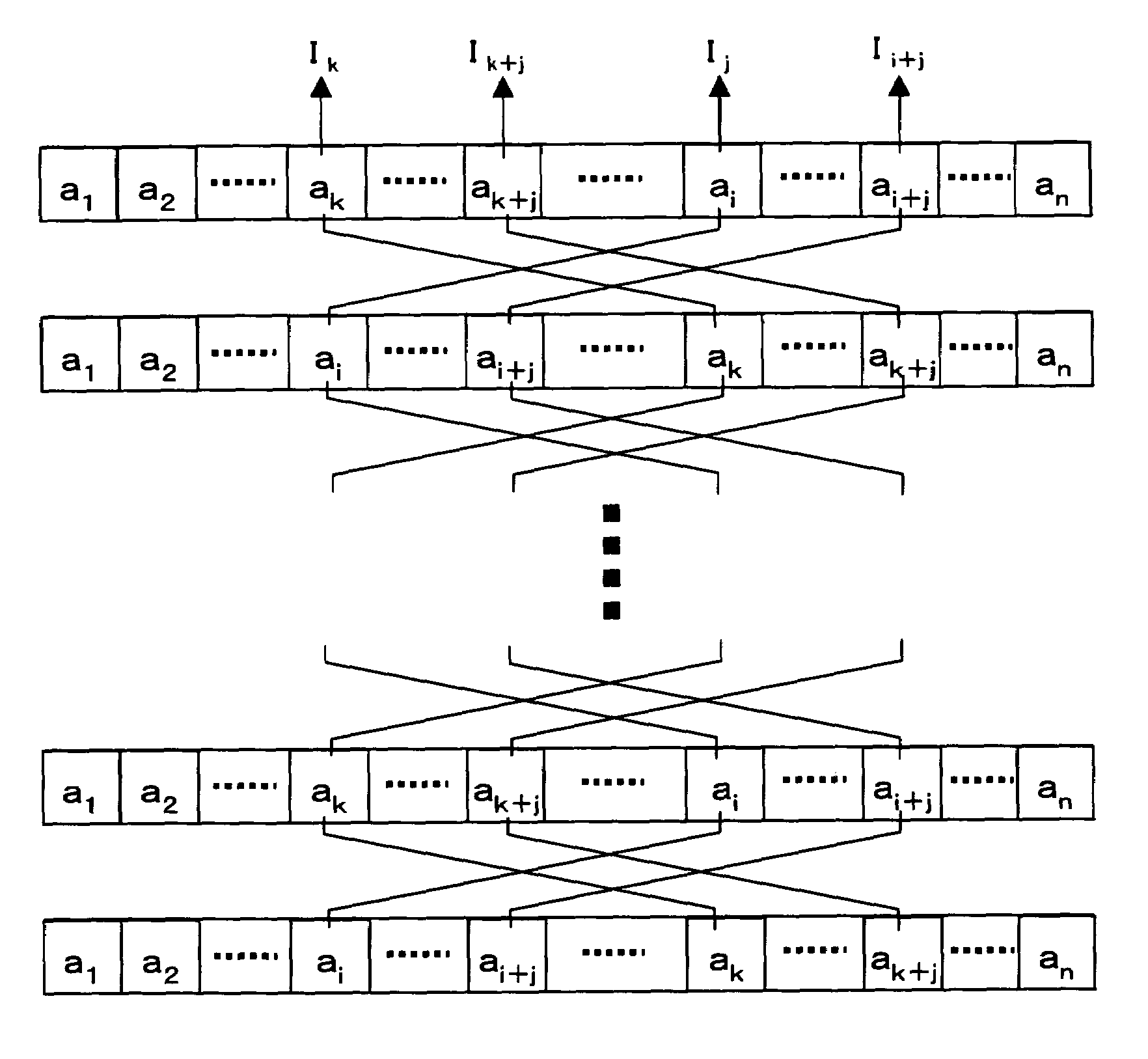
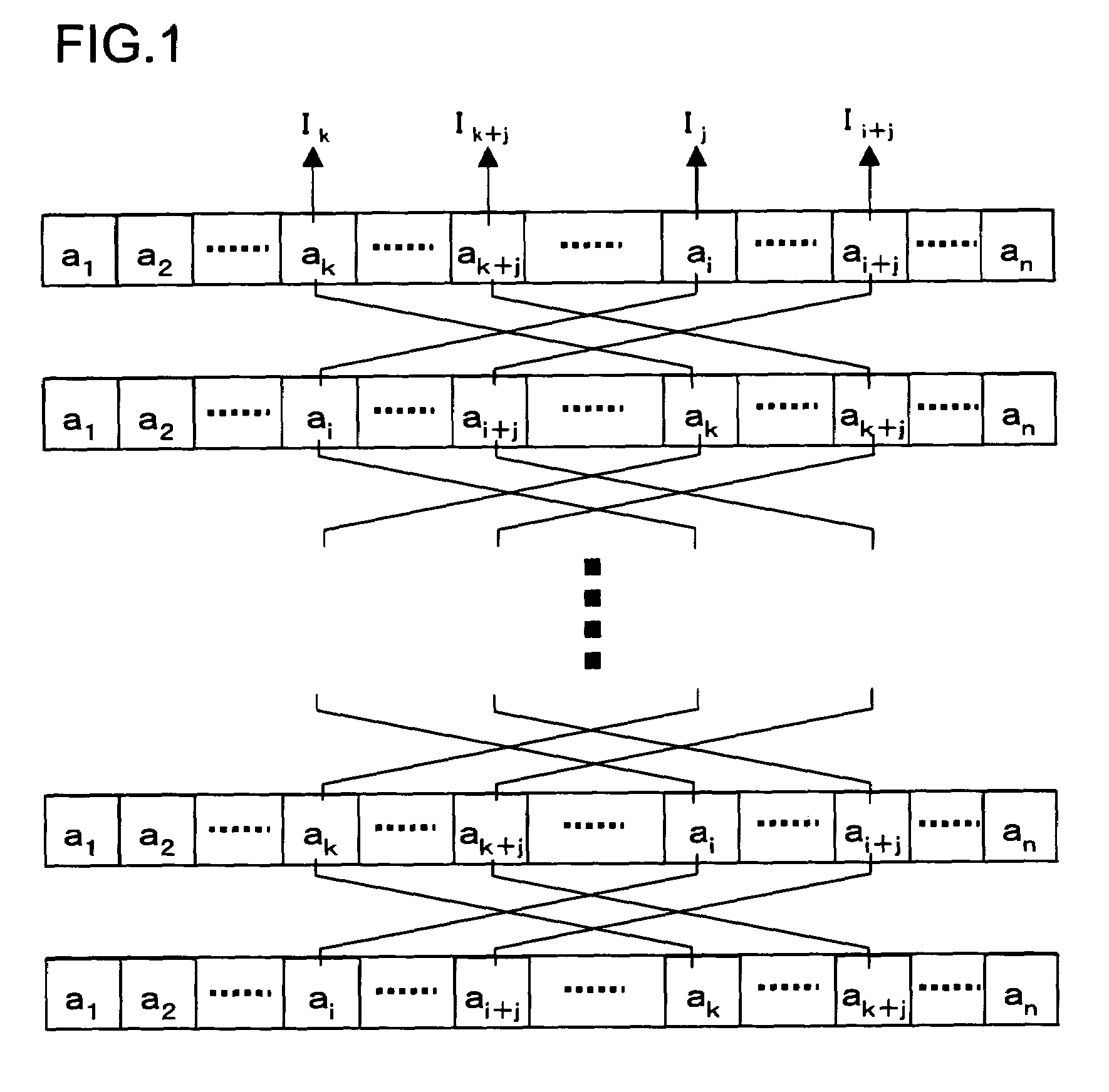
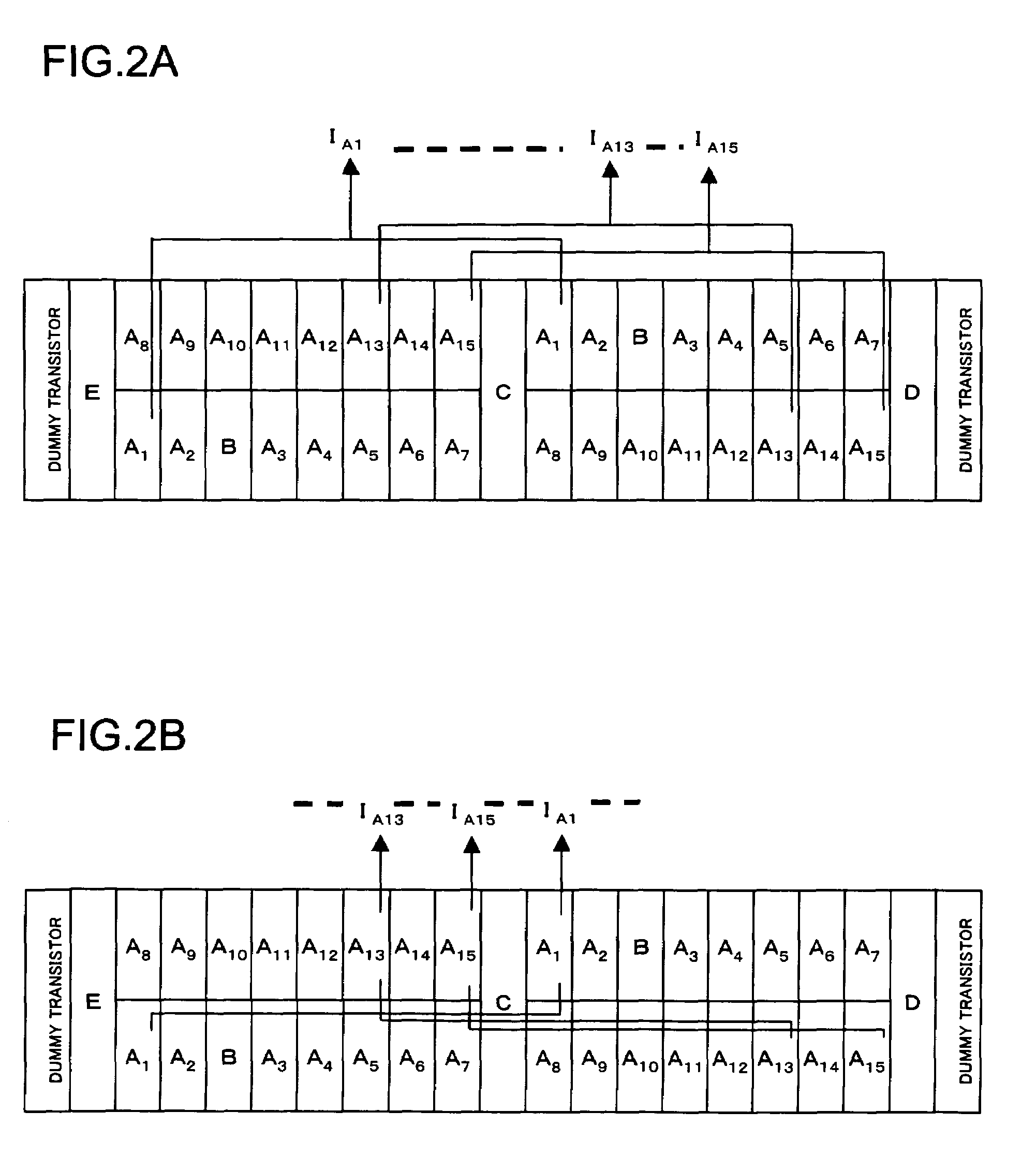
The present invention provides a current source cell arrangement that takes into account both slope-like and mountain-like variations in the manufacturing process. By considering these variations, the arrangement structure can be applied to a wider range of layouts and improve the performance of the current source cells. The current source cells are arranged in a two-dimensional matrix with a plurality of rows and columns, and each cell is labeled with a letter. The arrangement structure includes a first kind of row and a second kind of row, which are in the same order as the cells in the row. The current source cells in each column with a same letter from the first kind of row are connected one by one throughout all the rows. This arrangement structure is particularly useful for providing a high accuracy current source converter as a macro cell.

Problems solved by technology

In this case, although a linearity error is small, the number of switches SW1-SWn becomes as extremely large as 1,023, which makes implementation difficult.
However, in practice, the output current value from each current source cell is not constant, because there is a variation in transistor characteristics originated from the manufacturing process.
Therefore, a differential linearity error or a non-linearity (integral linearity) error occurs during the D / A conversion.

Method used


Image

  • Current source cell arrangement and digital-to-analog converter
  • Current source cell arrangement and digital-to-analog converter
  • Current source cell arrangement and digital-to-analog converter

Examples


Embodiment Construction

[0038]FIG. 1 shows a current source cell arrangement according to an example of the present invention. In FIG. 1, a1 through an where n is an integer equal to or larger than 4 represent current source cells, each of which is composed of a MOS transistor and the like to output a constant current. These current source cells are arranged in two-dimensional matrix on a semiconductor chip, a plurality of which are connected to form a current source cell arrangement that has a predetermined current value. Current source cells in the first row (the bottom row in FIG. 1) of the two dimensional matrix are labeled with letters from a1 to an. A first kind of row is in the same order as this row. A second kind of row is obtained from the first kind of row by exchanging a series of elements being letters from ai to ai+j where both i and j are integers equal to or larger than 1 and i+j is an integer equal to or less than n / 2 with a series of elements being letters from ak to ak+j where k is an in...


PUM


Abstract

An object of the present invention is to form a highly accurate current source for D / A converters. Letters from a1 to an where n is at least 4 represent current source cells that output constant currents, each of which is composed of MOS transistors etc. These current source cells are arranged in two dimensional matrix and a plurality of these current source cells are connected to form a current source that has a predetermined current value. Current source cells in any one row of the two dimensional matrix are labeled with letters from a1 to an. A first kind of row is in the same order as this row. A second kind of row is obtained from the first kind of row by exchanging a series of elements being letters from ai to ai+j where both i and j are integers at least 1 and i+j is an integer not more than n / 2 with a series of elements being letters from ak to ak+j where k is an integer larger than n / 2 and k+j is an integer not more than n. The two dimensional matrix comprises a same number of these two kinds of row.

Description

FIELD OF THE INVENTION[0001]The present invention relates to a current source cell arrangement and a digital-to-analog (D / A) converter, and more specifically to a current source cell arrangement that reduces influences of variations in characteristics of transistors resulting from manufacturing processes and a D / A converter equipped with the current source cell arrangement.BACKGROUND OF THE INVENTION[0002]A current addition type D / A converter that converts a digital signal to an analog signal is known. The current addition type D / A converter determines a number of current source cells selected based on a digital signal and adds up output current values of the selected current source cells to output an analog signal.[0003]FIG. 5 is a block diagram showing a configuration of the current addition type D / A converter. In FIG. 5, a digital signal Din is decoded by a decoder 110 to switch on and off switches SW1 through SWn. Each current output from current source cells 120 respectively is...

Claims


Application Information

Patent Timeline
Patent Type & Authority Patents(United States)
IPC IPC(8): H03M1/66
CPCH03M1/066H03M1/742
Inventor SHIMAYA, HIROSHI
Owner RENESAS ELECTRONICS CORP
Features
  • R&D
  • Intellectual Property
  • Life Sciences
  • Materials
  • Tech Scout
  • Unparalleled Data Quality
  • Higher Quality Content
  • 60% Fewer Hallucinations
Learn More