Apparatus and method for switching, modulation and dynamic control of light transmission using photonic crystals

a technology of photonic crystals and apparatuses, applied in the field of integrated electrooptical modulators, can solve the problems of lowering the optical loss of such a device, placing constraints on achieving, and design concerns that have not been adequately considered previously, so as to reduce power consumption and mitigate heating generation

Active Publication Date: 2008-09-02
OMEGA OPTICS
View PDF3 Cites 43 Cited by
  • Summary
  • Abstract
  • Description
  • Claims
  • Application Information

AI Technical Summary

Benefits of technology

The invention is about a device that can reduce power consumption and prevent overheating in integrated optics circuits. It is designed to improve the performance of electro-optical modulators.

Problems solved by technology

The technical problem addressed in this patent is the need for an electro-optical modulator that is ultra-compact, has low heat generation, and can operate at high speeds for use in optical communication and interconnection applications. The invention proposes a design that utilizes photonic crystals and modulation of refractive indices through the proper electrical structure to achieve these goals.

Method used


Image

  • Apparatus and method for switching, modulation and dynamic control of light transmission using photonic crystals
  • Apparatus and method for switching, modulation and dynamic control of light transmission using photonic crystals
  • Apparatus and method for switching, modulation and dynamic control of light transmission using photonic crystals

Examples


Embodiment Construction

[0033]Detailed descriptions of the preferred embodiment are provided herein. It is to be understood, however, that the present invention may be embodied in various forms. Therefore, specific details disclosed herein are not to be interpreted as limiting, but rather as a basis for the claims and as a representative basis for teaching one skilled in the art to employ the present invention in virtually any appropriately detailed system, structure or manner.

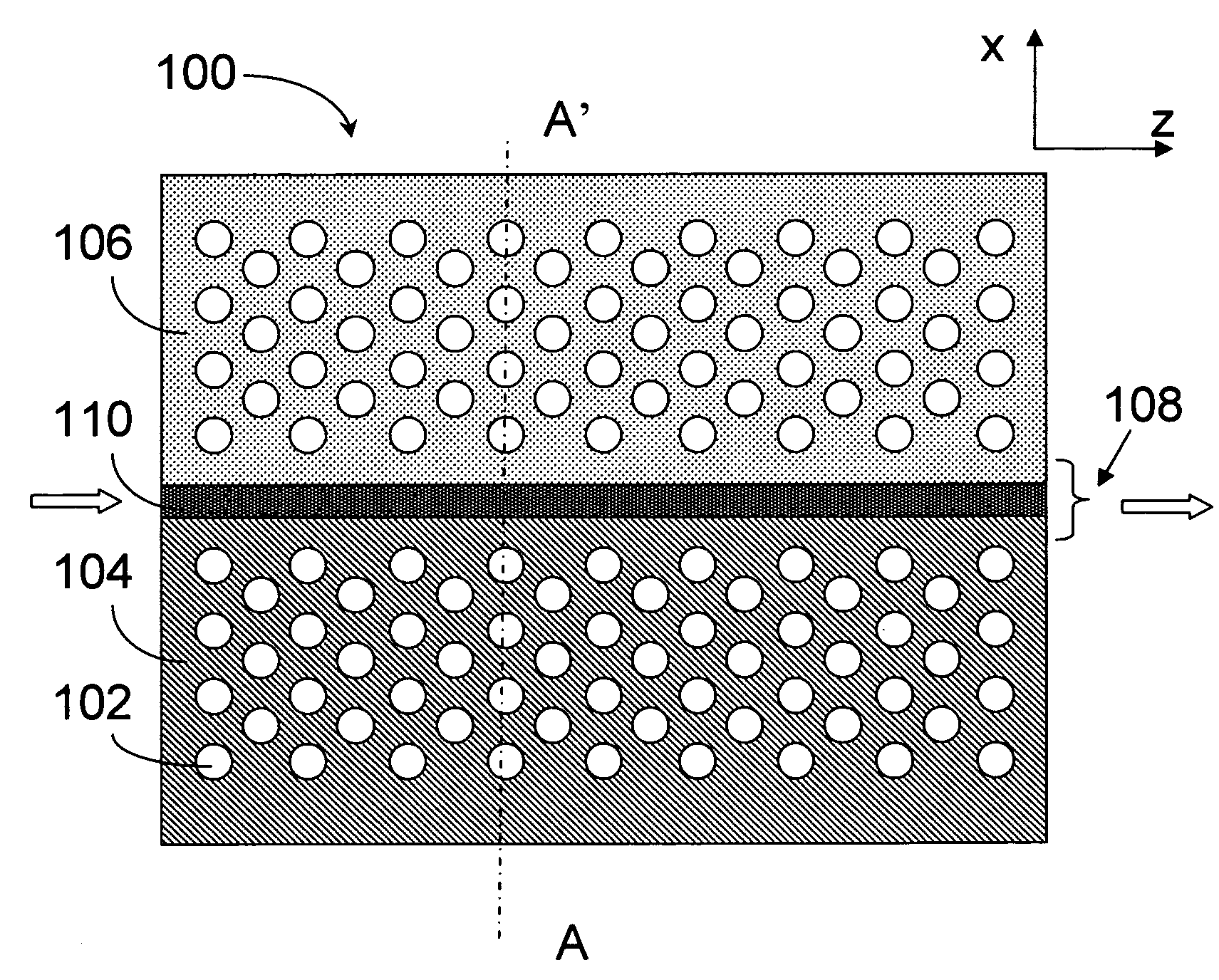
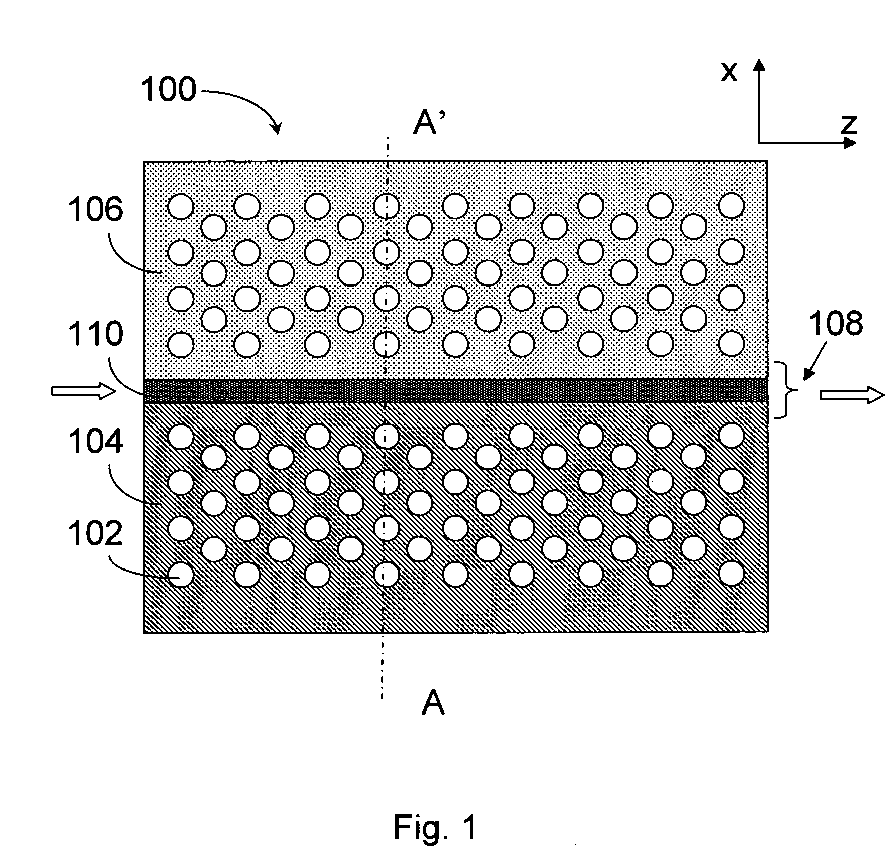
[0034]While integrated electronic circuits have undergone numerous generation of device miniaturization in last few decades, integrated optical devices have seen relatively less prominent progress in this regard. Particularly, the length of conventional integrated optical modulators remains around a few millimeters to a few centimeters. Photonic crystal emerged in recent years as a promising technology for miniaturization of integrated optical devices. Although it was known theoretically that a photonic crystal waveguide based Mach-Z...


PUM


Abstract

An active device for dynamic control of the transmission properties has at least one photonic crystal waveguide that has an electrically insulating layer formed within or near the waveguide core and two lateral conductive regions divided by the insulating layer. An alternating voltage signal induces phase and amplitude changes of electromagnetic wave propagating inside the device. Electromagnetic wave signals propagating through two such active photonic crystal waveguide devices may be mixed to produce at least one output signal through interference. Devices having one or more such active photonic crystal waveguides may be utilized as a tunable optical delay line, a tunable optical filter, a switch, or a modulator. A preferred embodiment comprises a photonic crystal waveguide made of a silicon slab with a periodic array of apertures or oxide columns therein, wherein an silicon oxide layer disposed in the waveguide core separates a p-doped region from an n-doped region.

Description


Claims


Application Information

Patent Timeline
Owner OMEGA OPTICS
Why Eureka
Try Eureka